KA9259D 데이터 시트보기 (PDF) - Fairchild Semiconductor
부품명
상세내역
일치하는 목록
KA9259D Datasheet PDF : 15 Pages
| |||
Application Information
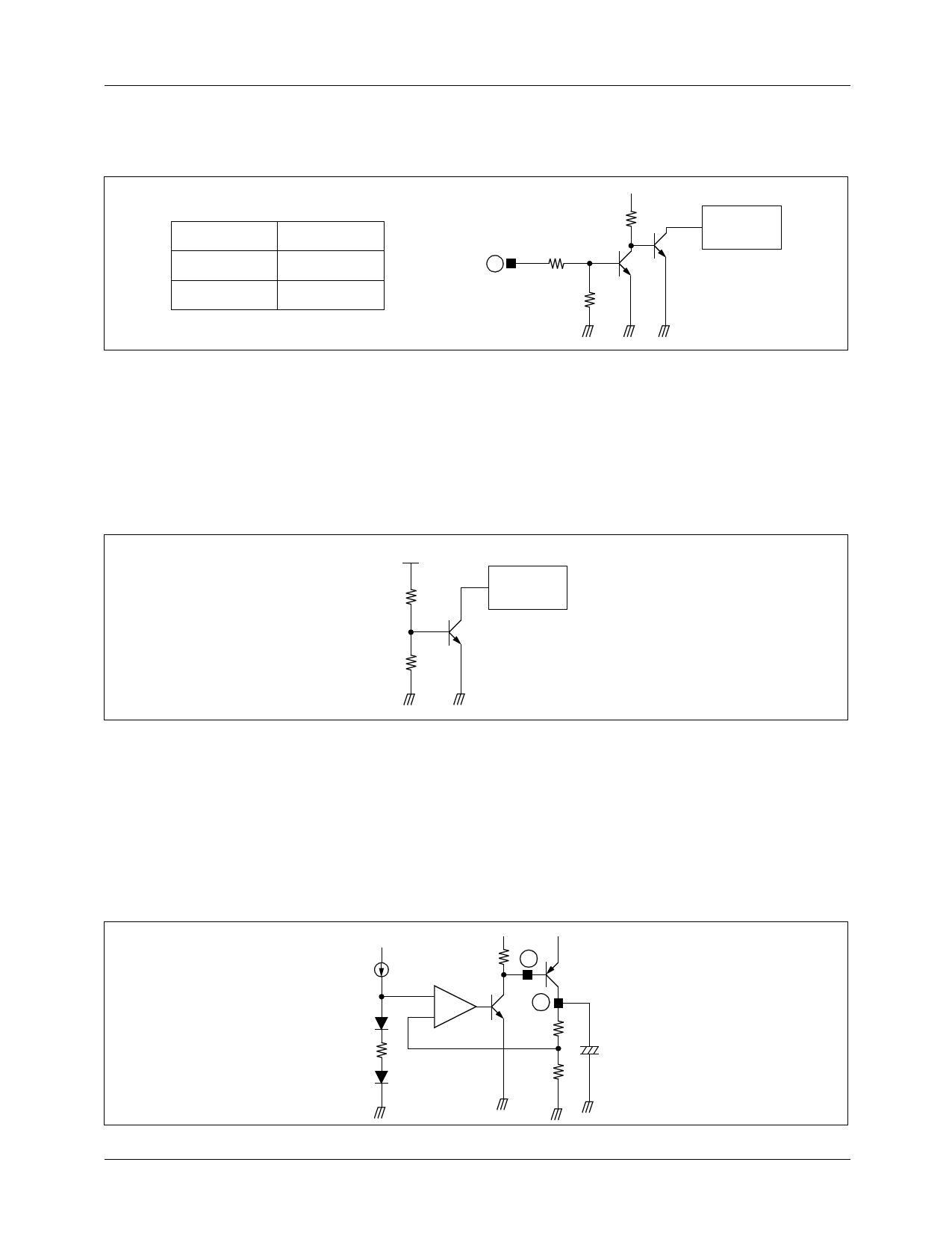
1. MUTE
KA9259D
Pin #7
Mute circuit
High
Turn-off
7
Low
Turn-on
Output driver
bias
• When the mute pin #7 is open or the voltage of the mute pin #7 is below 0.5V, the mute circuit is activated so that the output
circuit will be muted.
• When the voltage of the mute pin is above 2V, the mute circuit is disabled and the output circuit operates normal.
• If the chip temperature rises above 175°C, then the TSD (Thermal shutdown) circuit is activated and the output circuit is
muted.
2. TSD (THERMAL SHUTDOWN)
VREF BG
R11
Output driver
bias
Q11
R12
• The VREF BG is the output voltage of the band-gap-referenced biasing circuit and acts as the input voltage of the TSD
circuit.
• The base-emitter voltage of the TR, Q11 is designed to turn-on at below voltage.
VBE = VREF BG × R12 / (R11+R12) = 400mV
• When the chip temperature rises up to 175°C, then the turn-on voltage of the Q11 would drop down to 400mV.
Hence, the Q11 would turn on so the output circuit will be muted.
3. REGULATOR
I
VREF BG
−
+
D1
R1
D2
5
KSB772
6
VOUT
(5V)
R2
+
CE
R3
100µF
8
Share Link: 