KA9259D 데이터 시트보기 (PDF) - Fairchild Semiconductor
부품명
상세내역
일치하는 목록
KA9259D Datasheet PDF : 15 Pages
| |||
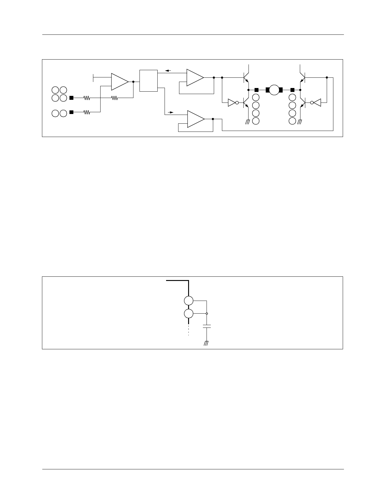
6. DRIVER (EXCEPT FOR LOADING MOTOR DRIVER)
KA9259D
3 10
19 25
4 24
VREF
(2.5V)
10k
100k
AMP
+
−
10k
Level
shift
−∆I + Buffer
−
+∆I
Buffer
+
−
Q1 −∆V
+∆V Q2
M
1
2
11
Q3 17
12
18 Q4
27
26
• The voltage, VREF, is the reference voltage given by the bias voltage of the pin #23.
• The input signal through the pin #3 is amplified by 10k/10k times and then fed to the level shift.
• The level shift produces the current due to the difference between the input signal and the arbitrary reference signal. The
current produced as +∆I and −∆I is fed into the driver buffer.
• Driver Buffer operates the power Transistor of the output stage according to the state of the input signal.
• The output stage is the BTL Driver and the motor is rotating in forward direction by operating TR Q1 and TR Q4. On the
other hand, if TR Q2 and TR Q3 is operating, the motor is rotating in reverse direction.
• When the input voltage through the pin #3 is below the VREF, then the direction of the motor in forward direction.
• When the input voltage through the pin #3 is above the VREF, then the direction of the motor in reverse direction.
• If it is desired to change the gain, then the pin #4 or #24 can be used.
7. When the bias voltage of the pin #23 is below 1.4V, then the output circuit is muted.
Hence for the normal operation, the bias voltage should be used in 1.6V~6.5V.
8. Connect a by-pass capacitor, 0.1µF between the supply voltage source.
VCC2 22
VCC1 21
104
9. Radiation fin is connecting to the internal GND of the package.
Connect the fin to the external GND.
10
Share Link: 