KA9259D 데이터 시트보기 (PDF) - Fairchild Semiconductor
부품명
상세내역
일치하는 목록
KA9259D Datasheet PDF : 15 Pages
| |||
KA9259D
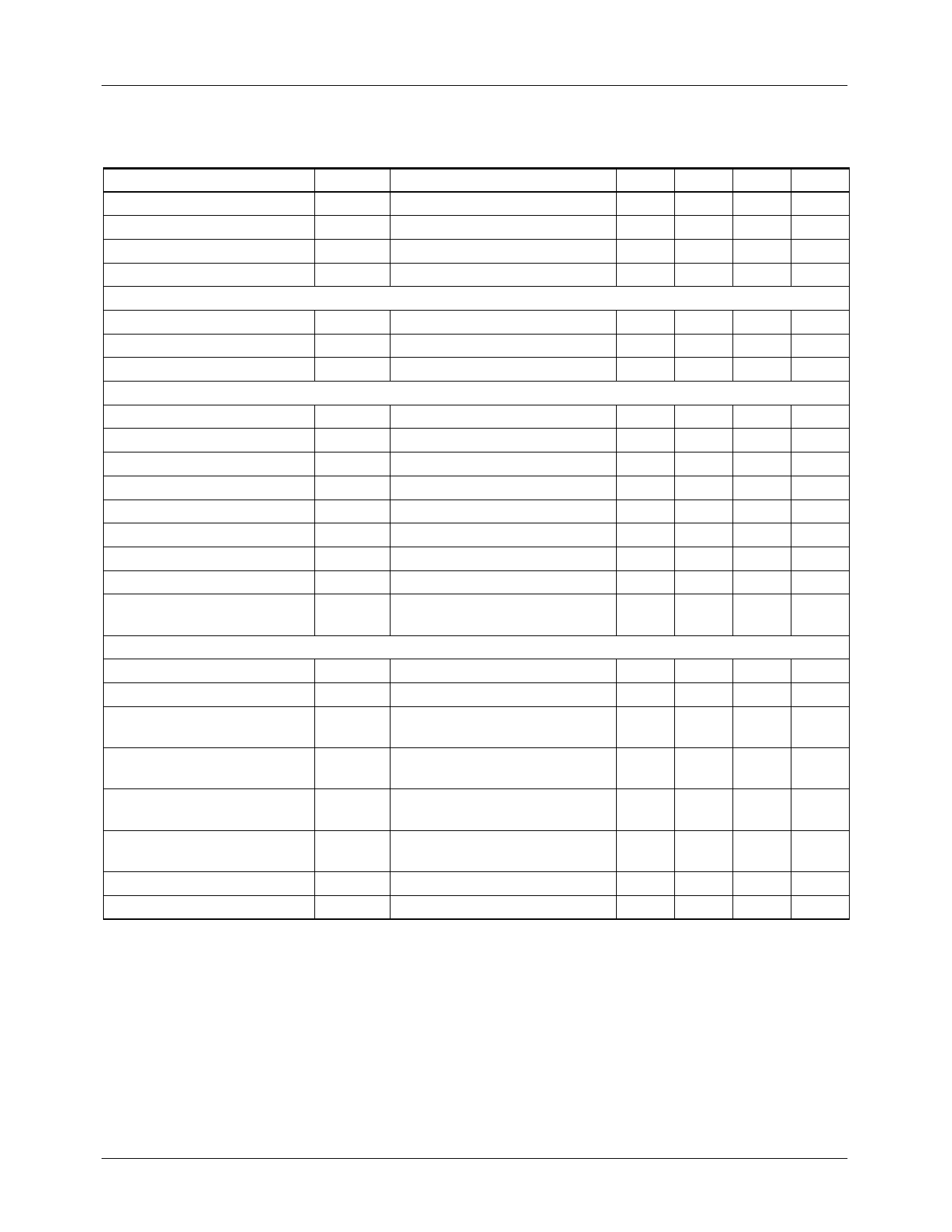
Electrical Characteristics
(Ta=25°C, VCC=8V, RL=8Ω, f=1kHz, unless otherwise specified)
Parameter
Symbol
Conditions
Min.
Quiescent circuit current
ICCQ Under no-load
2.5
Mute-on current
IMUTE Pin 7=GND
-
Mute-on voltage
VMON
-
-
Mute-off voltage
VMOFF
-
2
REGULATOR PART
Output voltage
VREG IL=100mA
4.7
Load regulation
∆VRL3 IL=0→200mA
−50
Line regulation
∆VCC VCC=6→13V, IL=100mA
−20
DRIVER PART (Except for loading motor driver)
Input offset voltage
VIO
-
−15
Output offset voltage 1
VOO1
-
−40
Maximum source current 1
Maximum sink current 1
ISOURCE1 RL=8Ω→VCC
ISINK1 RL=8Ω→GND
0.25
0.25
Maximum output voltage 1
VOM1 VIN=0.7V
2.5
Maximum output voltage 2
VOM2 VIN=7V
-
Closed-loop voltage gain
AVF VIN=0.1VRMS
5
Ripple rejection ratio
RR VIN=0.1VRMS, f=120Hz
40
Slew rate
SR 120Hz, VIN=1VRMS,
1
Square wave
LOADING MOTOR DRIVER PART (Unless otherwise specified, VCTL=open)
Output voltage 1
VO1 VPIN9=5V, VPIN14=0V, RL=45Ω 2.5
Output voltage 2
Output voltage regulation 1
(CTL)
VO2 VPIN9=0V, VPIN14=5V, RL=45Ω 2.5
VOCTL1 VCTL=3.5→4.5V, VPIN9=5V
0.5
VPIN14=0V, RL=45Ω
Output voltage regulation 2 VOCTL2 VCTL=3.5→4.5V, VPIN9=0V
0.5
(CTL)
VPIN14=5V, RL=45Ω
Load regulation 1
∆VRL1 IL=100→400mA, VPIN9=5V,
-
VPIN14=0V
Load regulation 2
∆VRL2 IL=100→400mA, VPIN9=0V,
-
VPIN14=5V
Output offset voltage 2
VOO2 VPIN9=5V, VPIN14=5V
−40
Output offset voltage 3
VOO3 VPIN9=0V, VPIN14=0V
−40
Typ.
6
2.5
-
-
5.0
0
0
-
-
0.4
0.4
3.3
−4.5
6.5
60
2
3.1
3.1
1.0
1.0
300
300
-
-
Max.
10
5
0.5
-
Units
mA
mA
V
V
5.3
V
50
mV
80
mV
15
mV
40
mV
-
A
-
A
-
V
−3.7
V
8
dB
-
dB
- V / µs
3.8
V
3.8
V
1.5
V
1.5
V
700 mV
700 mV
40
mV
40
mV
7
Share Link: 