ADG428 데이터 시트보기 (PDF) - Analog Devices
부품명
상세내역
일치하는 목록
ADG428 Datasheet PDF : 12 Pages
| |||
TERMINOLOGY
VDD
Most positive power supply potential.
VSS
Most negative power supply potential in dual
supplies. In single supply applications, it may
be connected to ground.
GND
Ground (0 V) reference.
RON
∆RON
Ohmic resistance between D and S.
Difference between the RON of any two
channels.
IS (OFF)
ID (OFF)
ID, IS (ON)
Source leakage current when the switch is off.
Drain leakage current when the switch is off.
Channel leakage current when the switch is
on.
VD (VS)
CS (OFF)
Analog voltage on terminals D, S.
Channel input capacitance for “OFF”
condition.
CD (OFF)
Channel output capacitance for “OFF”
condition.
CD, CS (ON)
CIN
tON (EN)
“ON” switch capacitance.
Digital input capacitance.
Delay time between the 50% and 90% points
of the digital input and switch “ON”
condition.
tOFF (EN)
Delay time between the 50% and 90% points
of the digital input and switch “OFF”
condition.
tTRANSITlON
Delay time between the 50% and 90% points
of the digital inputs and the switch “ON”
condition when switching from one address
state to another.
tOPEN
“OFF” time measured between 80% points of
both switches when switching from one
address state to another.
VINL
VINH
IINL (IINH)
Crosstalk
Maximum input voltage for Logic “0.”
Minimum input voltage for Logic “1.”
Input current of the digital input.
A measure of unwanted signal which is
coupled through from one channel to another
as a result of parasitic capacitance.
Off Isolation
A measure of unwanted signal coupling
through an “OFF” channel.
Charge
Injection
A measure of the glitch impulse transferred
from the digital input to the analog output
during switching.
IDD
Positive supply current.
ISS
Negative supply current.
ADG428/ADG429
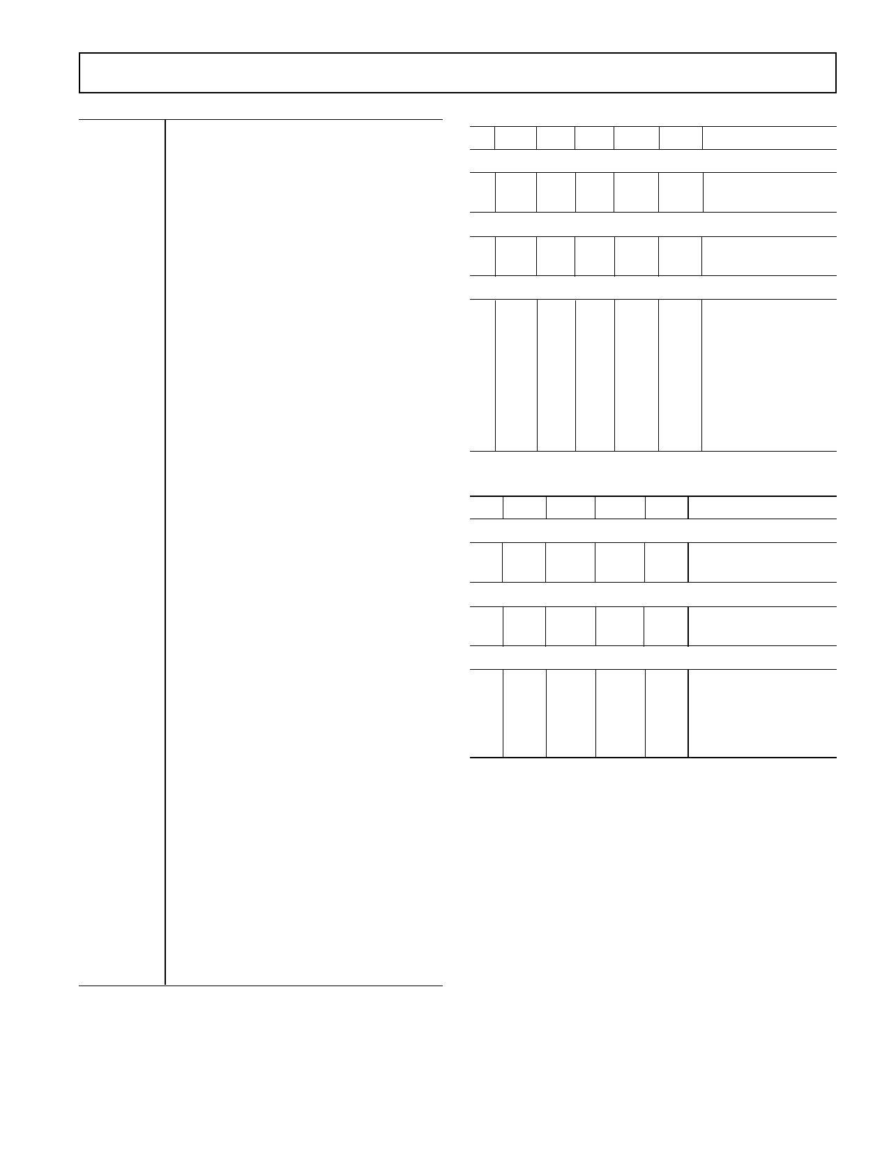
ADG428 Truth Table
A2 A1 A0 EN WR RS ON SWITCH
Latching
XXXXg 1
Maintains Previous
Switch Condition
Reset
XXXXX0
NONE
(Latches Cleared)
Transparent Operation
XXX0 0 1
000101
001101
010101
011101
100101
101101
110101
111101
NONE
1
2
3
4
5
6
7
8
ADG429 Truth Table
A1 A0 EN WR RS ON SWITCH PAIR
Latching
X
X
X
g
1
Maintains Previous
Switch Condition
Reset
X
X
X
X
0
NONE
(Latches Cleared)
Transparent Operation
X
X
0
0
1
NONE
0
0
1
0
1
1
0
1
1
0
1
2
1
0
1
0
1
3
1
1
1
0
1
4
REV. C
–5–
Share Link: 