ICS9250-29 데이터 시트보기 (PDF) - Integrated Circuit Systems
부품명
상세내역
일치하는 목록
ICS9250-29 Datasheet PDF : 15 Pages
| |||
ICS9250-29
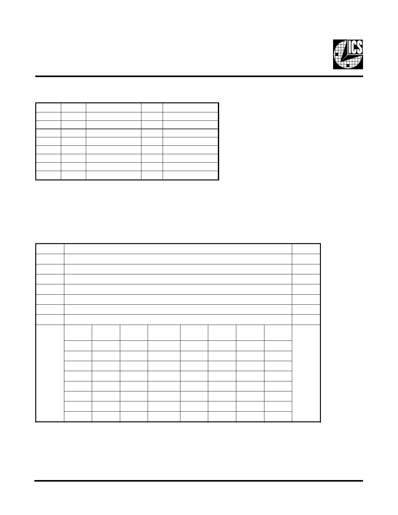
Byte 2: Control Register
(1 = enable, 0 = disable)
Bit Pin#
Name
Bit 7 12 3V66_2 (AGP)
Bit 6 31 SDRAM12
Bit 5 34 SDRAM11
Bit 4 35 SDRAM10
Bit 3 38 SDRAM9
Bit 2 39 SDRAM8
Bit 1 15 PCICLK1
Bit 0 - Undefined bit
PWD Description
1 (Active / Inactive )
1 (Active / Inactive )
1 (Active / Inactive )
1 (Active / Inactive )
1 (Active / Inactive )
1 (Active / Inactive )
1 (Active / Inactive )
0 (Active / Inactive )
Notes:
1. Inactive means outputs are held LOW and are disabled from switching. These outputs are designed to be configured at
power-on and are not expected to be configured during the normal modes of operation.
2. PWD = Power on Default
3. Undefined bits can be written with either "1" or "0"
Byte 3: ICS Reserved Functionality and frequency select register (Default as noted in PWD)
Bit
Bit 7
Bit 6
Bit 5
Bit 4
Bit 3
Bit 2
Bit 1
Bit 0
Description
ICS Reserved bit (Note 2)
ICS Reserved bit (Note 2)
ICS Reserved bit (Note 2)
ICS Reserved bit (Note 2)
5% overclock mode (1 = 5% / 0= normal )
Undefined bit (note 3)
Tristate#/PWRDN# ( 1 = PWRDN# / 0 = Tristate# ) see pin description
Bit 0
FS1
FS0
CPUCLK SDRAM 3V66 PCICLK IOAPIC
MHz MHz MHz MHz MHz
0
0
0
66.66 100.0 66.66 33.33 33.33
0
0
1
100.0 100.0 66.66 33.33 33.33
0
1
0
133.32 133.32 66.66 33.33 33.33
0
1
1
133.32 100.0 66.66 33.33 33.33
1
0
0
66.66 100.0 66.66 33.33 33.33
1
0
1
100.0 100.0 66.66 33.33 33.33
1
1
0
133.32 133.32 66.66 33.33 33.33
1
1
1
133.32 133.32 66.66 33.33 33.33
PWD
0
0
0
0
0
1
1
0
Note 1
Note 1: For system operation, the BSEL lines of the CPU will program FS0, FS1 for the appropriate CPU speed, always with
SDRAM = 100MHz. After BIOS verifies the SDRAM is PC133 speed, then bit 0 can be written from the default 0 to 1
to change the SDRAM output frequency from 100MHz to 133MHz. This will only change if the CPU is at the
133MHz FSB speed as shown in this table. The CPU, 3V66, PCI and IOAPIC clocks will be glitch free during this
transition, and only SDRAM will change.
Note 2: Must be written with "0"
Note 3: Undefined bits can be written with either "1" or "0"
6
Share Link: 