AN-6921 데이터 시트보기 (PDF) - Fairchild Semiconductor
부품명
상세내역
일치하는 목록
AN-6921
Fairchild Semiconductor

AN-6921 Datasheet PDF : 16 Pages
| |||
AN-6921
APPLICATION NOTE
(Design Example) Since the output voltage is 400V for
high line and 260V for low line, the minimum
frequency occurs at high-line (264VAC) and full-load
condition. Assuming the overall efficiency is 90% and
selecting the minimum frequency as 58kHz, the
inductor value is obtained as:
L = η ⋅VLINE,MAX 2 ⋅ VO.PFC.H − 2VLINE,MAX
2 ⋅ POUT ⋅ fSW ,MIN
VO . PFC . H
= 0.9 ⋅ 2642 ⋅ 400 − 2 ⋅ 264 = 400μ H
2 ⋅ 90 ⋅ 58×103
400
The maximum peak inductor current at nominal
output power is calculated as:
I L,PK
= 2 2 ⋅ POUT
η ⋅VLINE,MIN
= 2 2 ⋅90 = 3.14A
0.9 ⋅ 90
t MAX
ON
= 2 ⋅ POUT ⋅ L
η ⋅VLINE.MIN 2
=
2 ⋅ 90 ⋅ 400 ×10−6
0.9 ⋅ 902
= 9.87μs < 20μs
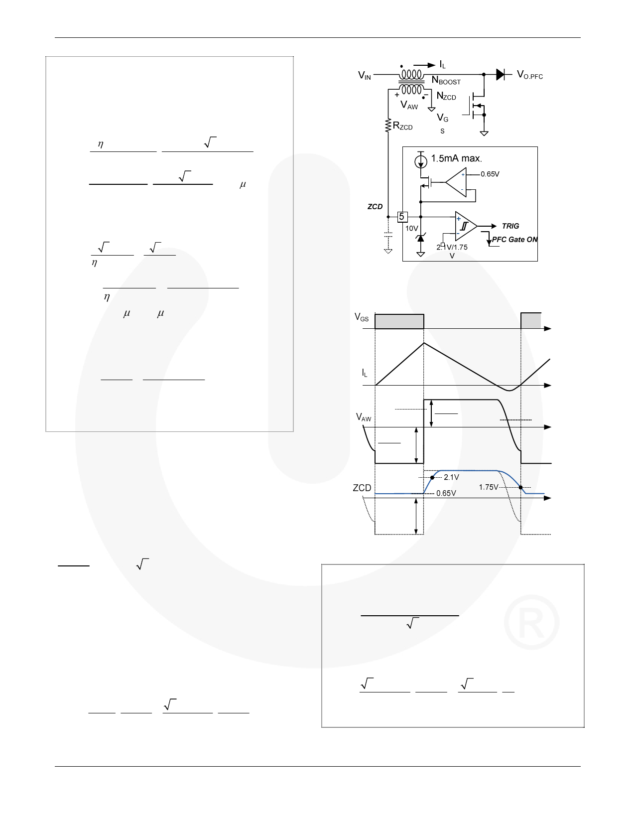
Figure 8. Internal Block for ZCD
Assuming RM10 core (PC40, Ae=98mm2) is used and
setting ΔB as 0.23T, the primary winding should be:
N BOOST
≥
IL,PK ⋅ L
Ae ⋅ ΔB
=
3.14 ⋅ 400 ×10−6
98×10−6 ⋅ 0.23
= 55.7 turns
Thus, the number of turns (NBOOST) of boost inductor is
determined as 60.
[STEP-A2] Auxiliary Winding Design
Figure 9 shows the internal block for zero-current detection
(ZCD) for the PFC. FAN6921 indirectly detects the inductor
zero current instant using an auxiliary winding of the boost
inductor.
The auxiliary winding should be designed such that the
voltage of the ZCD pin rises above 2.1V when the boost
switch is turned off to trigger internal comparator as:
N ZCD
N BOOST
(VO.PFC.H
−
2VLINE.MAX ) > 2.1V
(10)
where VO.PFC.H is the PFC output voltage for high line
condition.
The ZCD pin has upper voltage clamping and lower voltage
clamping at 10V and 0.65V, respectively. When the ZCD
pin voltage is clamped at 0.65V, the maximum sourcing
current is 1.5mA and, therefore, the resistor RZCD should be
properly designed to limit the current of the ZCD pin below
1.5mA in the worst case as:
RZCD
> VIN ⋅ N AUX
1.5mA NBOOST
=
2VLINE.MAX ⋅ N AUX
1.5mA NBOOST
(11)
N ZCD
N BOOST
VIN
NZCD
N BOOST
(VO.PFC
−VIN )
Figure 9. ZCD Waveforms
(Design Example) The number of turns for the auxiliary
ZCD winding is obtained as:
N ZCD
>
2.1N BOOST
(VO.PFC.H − 2VLINE.MAX
)
=
4.7turns
With a margin, NAUX is determined as 8 turns.
Then RZCD is selected from:
RZCD >
2VLINE.MAX
1.5mA
⋅ NZCD
N BOOST
=
2 ⋅ 265
1.5 ×10−3
⋅
8
60
=
33kΩ
as 68kΩ.
© 2010 Fairchild Semiconductor Corporation
Rev. 1.0.1 • 8/24/10
5
www.fairchildsemi.com
Share Link: