DG509B 데이터 시트보기 (PDF) - Vishay Semiconductors
부품명
상세내역
일치하는 목록
DG509B Datasheet PDF : 18 Pages
| |||
DG508B, DG509B
Vishay Siliconix
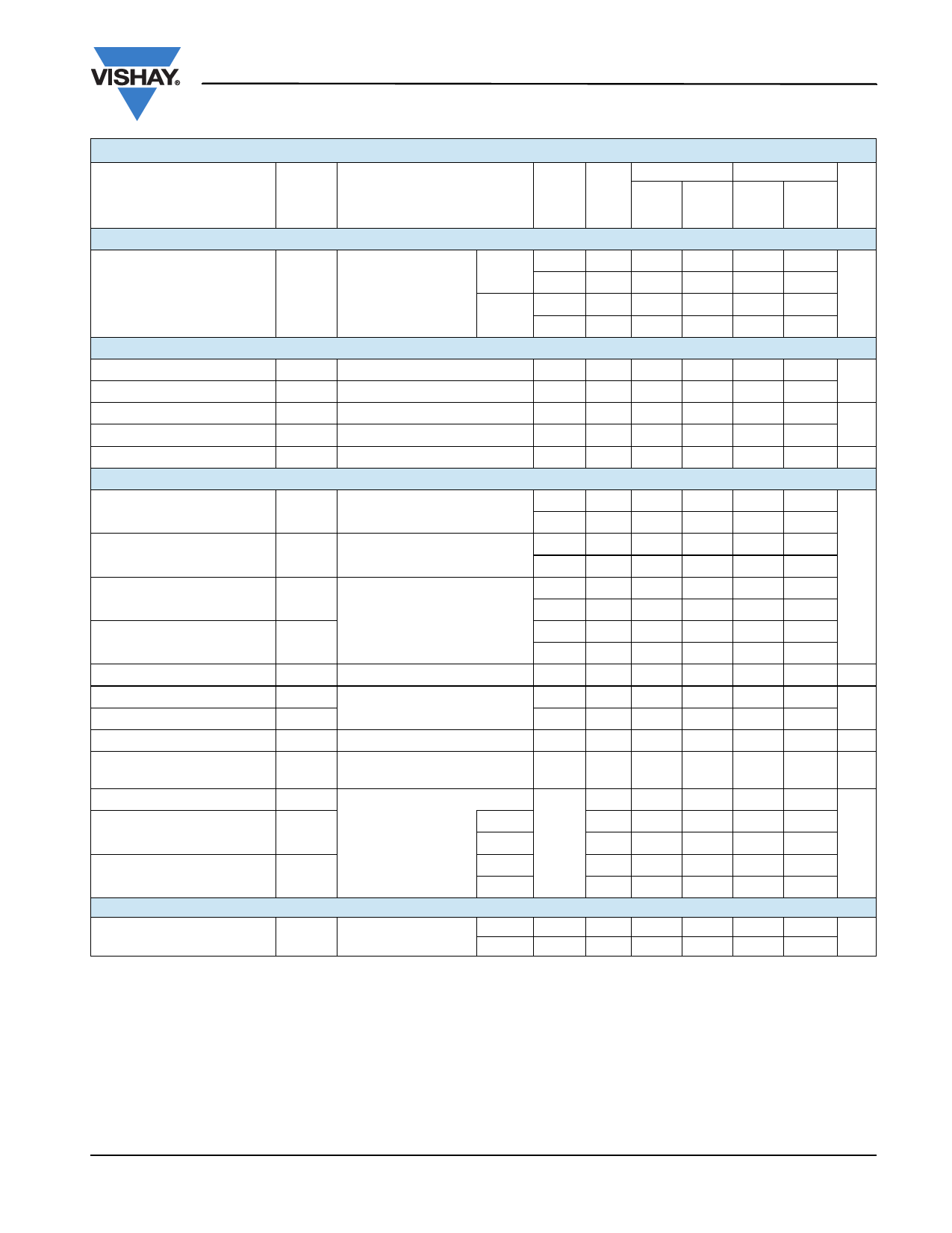
SPECIFICATIONS (Single Supply 12 V)
Parameter
Analog Switch
Symbol
Test Conditions
Unless Otherwise Specified
V+ = 12 V, V- = 0 V (± 10 %)
VAX, VEN = 2.0 V, 0.8 Va
- 40 °C to 125 °C - 40 °C to 85 °C
Temp.b Typ.c Min.d Max.d Min.d Max.d Unit
Channel On Leakage Current ID(on)
V+ = 12 V, V- = 0 V
VS = VD = 0 V/10 V
Room
DG508B
Full
Room
DG509B
Full
-1
1
-1
1
- 100 100 - 100 100
nA
-1
1
-1
1
- 50
50
- 50
50
Digital Control
Logic High Input Voltage
Logic Low Input Voltage
Logic High Input Current
Logic Low Input Current
Logic Input Capacitancee
Dynamic Characteristics
VINH
VINL
IIH
IIL
Cin
VAX, VEN = 2.0 V
VAX, VEN = 0.8 V
f = 1 MHz
Full
Full
Full
Full
Room 4
2.0
2.0
0.8
-1
1
-1
-1
1
-1
V
0.8
1
µA
1
pF
Transition Time
tTRANS
VS1 = 10 V/0 V, VS8 = 0 V/10 V, Room
RL = 1 M, CL = 35 pF
Full
165
400
550
400
500
Break-Before-Make Interval
tOPEN
VS1 = VS8 = 5 V, CL = 35 pF,
RL = 1 k
Room 37
Full
15
1
15
1
ns
Room 125
300
300
Enable Turn-On Time
tON(EN)
VS1 = 5 V, VS2 to VS8 = 0 V,
Full
550
425
RL = 1 k, CL = 35 pF
Room 75
250
250
Enable Turn-Off Time
tOFF(EN)
Full
350
300
Charge Injectione
Off Isolatione
Crosstalke
- 3 dB Bandwidthe
QINJ CL = 1 nF, RGEN = 0 , VGEN = 0 V Full
2.5
OIRR
XTALK
CL = 5 pF, RL = 50
f = 1 MHz
Room - 80
Room - 88
BW
RL = 50
Room 200
pC
dB
MHz
Total Harmonic Distortione
THD
RL = 10 k, 5 VRMS,
f = 20 Hz to 20 kHz
Room 0.26
%
Source Off Capacitancee
CS(off)
2
Drain Off Capacitancee
CD(off)
f = 1 MHz
DG508B
13
DG509B Room 8
pF
Channel On Capacitancee
CD(on)
DG508B
17
DG509B
12
Power Supply
Room 0.01
0.5
Power Supply Current
I+
VAX, VEN = 0 V, or V+
Full
0.6
0.5
mA
0.6
Notes:
a. VAX, VEN = input voltage perform proper function.
b. Room = 25 °C, Full = as determined by the operating temperature suffix.
c. Typical values are for DESIGN AID ONLY, not guaranteed nor subject to production testing.
d. The algebraic convention whereby the most negative value is a minimum and the most positive a maximum, is used in this datasheet.
e. Guaranteed by design, not subject to production test.
f. RDS(on) = RDS(on) max. - RDS(on) min.
Stresses beyond those listed under “Absolute Maximum Ratings” may cause permanent damage to the device. These are stress ratings only, and functional operation
of the device at these or any other conditions beyond those indicated in the operational sections of the specifications is not implied. Exposure to absolute maximum
rating conditions for extended periods may affect device reliability.
Document Number: 64821
S10-2817-Rev. D, 20-Dec-10
www.vishay.com
5
Share Link: 