DG509B 데이터 시트보기 (PDF) - Vishay Semiconductors
부품명
상세내역
일치하는 목록
DG509B Datasheet PDF : 18 Pages
| |||
DG508B, DG509B
Vishay Siliconix
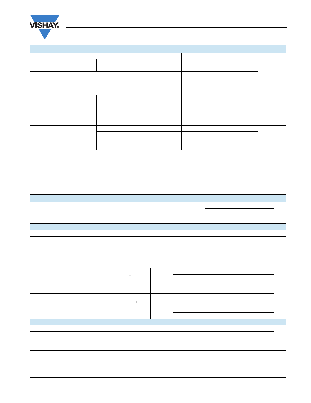
ABSOLUTE MAXIMUM RATINGS
Parameter
Limit
Unit
Voltages Referenced to V-
Digital Inputsa, VS, VD
V+
GND
44
25
V
(V-) - 2 to (V+) + 2
or 20 mA, whichever occurs first
Current (Any terminal)
Peak Current, S or D (Pulsed at 1 ms, 10 % duty cycle max.)
30
mA
100
Storage Temperature
Power Dissipation (Packages)b
Thermal Resistance (J-A)b
(EY, EQ, EJ, EN suffix)
16-Pin Narrow SOICc
16-Pin TSSOPd
16-Pin PDIPe
16-Pin miniQFNf
16-Pin Narrow SOICc
16-Pin TSSOPd
16-Pin PDIPe
16-Pin miniQFNf
- 65 to 150
600
450
510
525
125
178
159.6
152
°C
mW
°C/W
Notes:
a. Signals on SX, DX or INX exceeding V+ or V- will be clamped by internal diodes. Limit forward diode current to maximum current ratings.
b. All leads soldered or welded to PC board.
c. Derate 8.0 mW/°C above 70 °C.
d. Derate 5.6 mW/°C above 70 °C.
e. Derate 6.3 mW/°C above 70 °C.
f. Derate 6.6 mW/°C above 70 °C.
SPECIFICATIONS
Parameter
Analog Switch
Analog Signal Rangee
Drain-Source
On-Resistance
RDS(on) Matching
Symbol
VANALOG
RDS(on)
RDS(on)
Source Off Leakage Current IS(off)
Drain Off Leakage Current
ID(off)
Drain On Leakage Current
ID(on)
Digital Control
Logic High Input Voltage
Logic Low Input Voltage
Logic High Input Current
Logic Low Input Current
Logic Input Capacitancee
VINH
VINL
IIH
IIL
Cin
Test Conditions
Unless Otherwise Specified
V+ = 15 V, V- = - 15 V (± 10 %)
VAX, VEN = 2.0 V, 0.8 Va
- 40 °C to 125 °C - 40 °C to 85 °C
Temp.b Typ.c Min.d Max.d Min.d Max.d
Unit
Full
- 15
15
- 15
15
V
Room 180
380
VD = ± 10 V, IS = - 1 mA
Full
480
380
450
VD = ± 10 V
Room 10
Room
-1
1
-1
1
VD = ± 10 V
VS = 10 V
VEN = 0 V
DG508B
DG509B
Full
Room
Full
Room
Full
- 50
50
- 50
50
-1
1
-1
1
- 100 100 - 100 100
-1
1
-1
1
nA
- 50
50
- 50
50
VS = VD = 10
sequence each
switch on
DG508B
DG509B
Room
Full
Room
Full
-1
1
-1
1
- 100 100 - 100 100
-1
1
-1
1
- 50
50
- 50
50
VAX, VEN = 2.0 V
VAX, VEN = 0.8 V
f = 1 MHz
Full
Full
Full
Full
Room 4
2.0
2.0
0.8
-1
1
-1
-1
1
-1
V
0.8
1
µA
1
pF
Document Number: 64821
S10-2817-Rev. D, 20-Dec-10
www.vishay.com
3
Share Link: 