CY7C130 데이터 시트보기 (PDF) - Cypress Semiconductor
부품명
상세내역
일치하는 목록
CY7C130 Datasheet PDF : 19 Pages
| |||
CY7C130/CY7C131
CY7C140/CY7C141
Maximum Ratings[4]
(Above which the useful life may be impaired. For user guide-
lines, not tested.)
Storage Temperature ................................. –65°C to +150°C
Ambient Temperature with
Power Applied............................................. –55°C to +125°C
Supply Voltage to Ground Potential
(Pin 48 to Pin 24) ........................................... –0.5V to +7.0V
DC Voltage Applied to Outputs
in High Z State ............................................... –0.5V to +7.0V
DC Input Voltage............................................ –3.5V to +7.0V
Output Current into Outputs (LOW) .............................20 mA
Static Discharge Voltage........................................... >2001V
(per MIL-STD-883, Method 3015)
Latch-Up Current.................................................... >200 mA
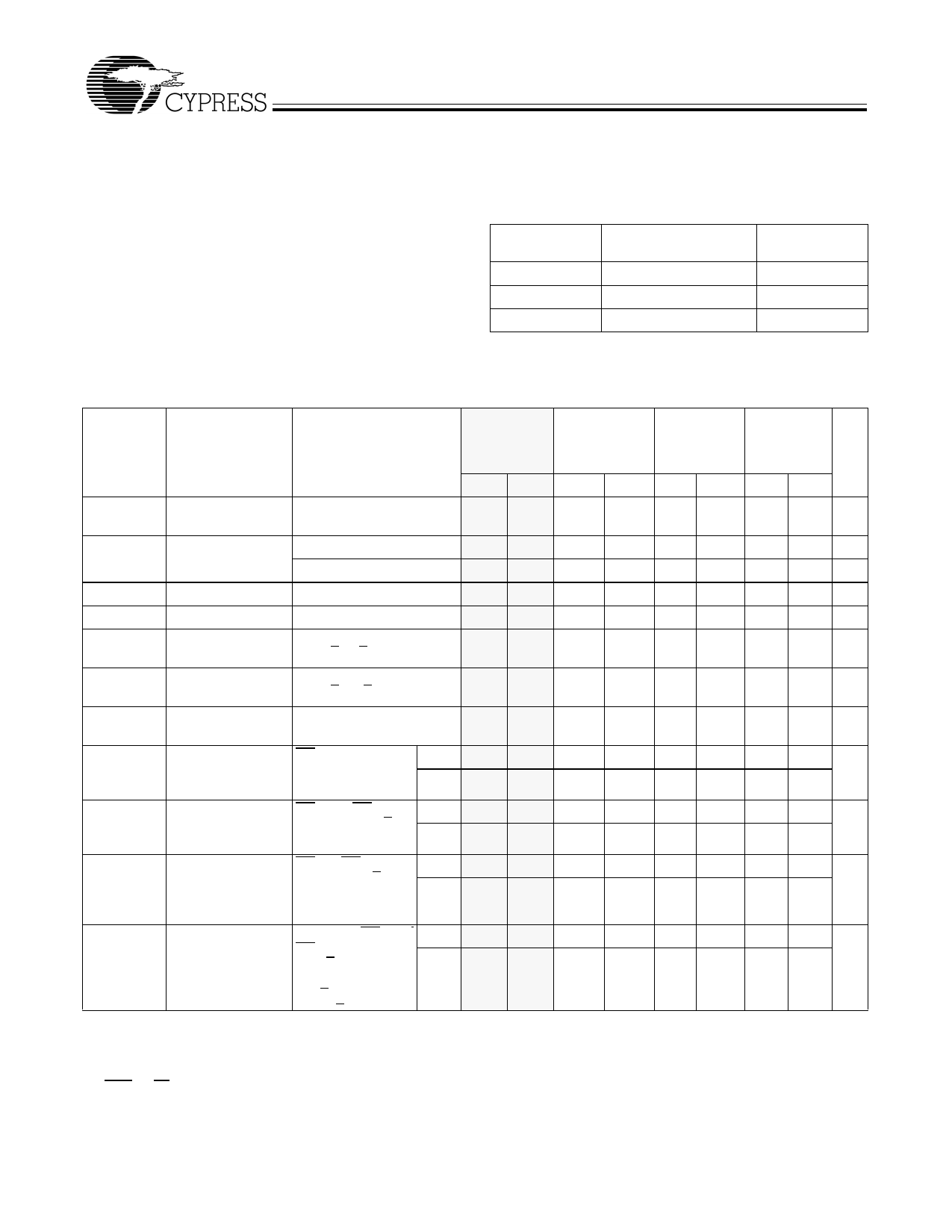
Operating Range
Range
Commercial
Industrial
Military[5]
Ambient
Temperature
0°C to +70°C
–40°C to +85°C
–55°C to +125°C
VCC
5V ± 10%
5V ± 10%
5V ± 10%
Electrical Characteristics Over the Operating Range[6]
7C131-15[3]
7C141-15
7C130-30[3]
7C131-25,30
7C140-30
7C141-25,30
7C130-35,45
7C131-35,45
7C140-35,45
7C141-35,45
7C130-55
7C131-55
7C140-55
7C141-55
Parameter Description
Test Conditions
Min. Max. Min. Max. Min. Max. Min. Max. Unit
VOH
Output HIGH
VCC = Min., IOH = –4.0 mA 2.4
2.4
2.4
2.4
V
Voltage
VOL
Output LOW
IOL = 4.0 mA
Voltage
IOL = 16.0 mA[7]
VIH
Input HIGH Voltage
VIL
Input LOW Voltage
IIX
Input Leakage
GND < VI < VCC
Current
IOZ
Output Leakage GND < VO < VCC,
Current
Output Disabled
0.4
0.4
0.4
0.4 V
0.5
0.5
0.5
0.5
2.2
2.2
2.2
2.2
V
0.8
0.8
0.8
0.8 V
–5 +5 –5 +5 –5 +5 –5 +5 µA
–5 +5 –5 +5 –5 +5 –5 +5 µA
IOS
Output Short
Circuit Current[8, 9]
VCC = Max.,
VOUT = GND
–350
ICC
VCC Operating
CE = VIL,
Com’l
190
Supply Current
Outputs Open,
f = fMAX[10]
Mil
ISB1
Standby Current
Both Ports,
TTL Inputs
CEL
VIH,
fa=ndfMCAEXR[10>]
Com’l
Mil
75
–350
170
65
–350
120
170
45
65
–350 mA
110 mA
120
35 mA
45
ISB2
Standby Current CEL or CER > VIH, Com’l
135
One Port,
TTL Inputs
Active Port Outputs
Open,
Mil
f = fMAX[10]
115
90
75 mA
115
90
ISB3
Standby Current Both Ports CEL and Com’l
15
Both Ports,
CMOS Inputs
CER >
VCC – 0.2V,
Mil
VIN > VCC – 0.2V
or VIN < 0.2V, f = 0
15
15
15 mA
15
15
Shaded areas contain preliminary information.
Note:
4. The Voltage on any input or I/O pin cannot exceed the power pin during power-up.
5. TA is the “instant on” case temperature
6. See the last page of this specification for Group A subgroup testing information.
7. BUSY and INT pins only.
8. Duration of the short circuit should not exceed 30 seconds.
9. This parameter is guaranteed but not tested.
10. At f = fMAX, address and data inputs are cycling at the maximum frequency of read cycle of 1/tRC and using AC Test Waveforms input levels of GND to 3V.
Document #: 38-06002 Rev. *D
Page 3 of 19
Share Link: 