CS8120YD14 데이터 시트보기 (PDF) - ON Semiconductor
부품명
상세내역
일치하는 목록
CS8120YD14 Datasheet PDF : 14 Pages
| |||
CS8120
CIRCUIT DESCRIPTION
VOLTAGE REFERENCE AND OUTPUT CIRCUITRY
Precision Voltage Reference
The regulated output voltage depends on the precision band
gap voltage reference in the IC. By adding an error amplifier
into the feedback loop, the output voltage is maintained
within ±4.0% over temperature and supply variation.
Output Stage
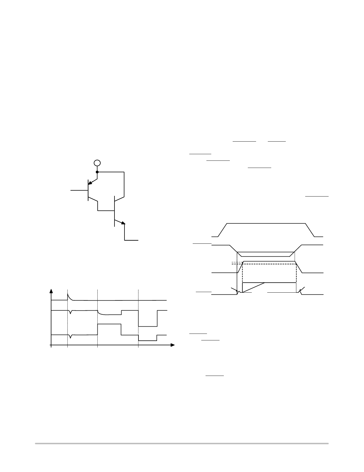
The composite PNP−NPN output structure (Figure 9)
provides 300 mA (Typ) of output current while maintaining
a low drop out voltage (1.00 V, Typ) and drawing little
quiescent current (2.5 mA). The NPN pass device prevents
deep saturation of the output stage which in turn improves
the IC’s efficiency by preventing excess current from being
used and dissipated by the IC.
VIN
circuitry and enables the IC to survive unexpected voltage
transients.
Using an emitter sense scheme, the amount of current
through the NPN pass transistor is monitored. Feedback
circuitry insures that the output current never exceeds a
preset limit.
Should the junction temperature of the power device
exceed 180°C (Typ) the power transistor is turned off.
Thermal shutdown is an effective means to prevent die
overheating since the power transistor is the principle heat
source in the IC.
REGULATOR CONTROL FUNCTIONS
The CS8120 contains two microprocessor compatible
control functions: ENABLE and RESET (Figure 11).
ENABLE Function
The ENABLE function switches the output transistor.
When the voltage on the ENABLE lead exceeds 2.9 V Typ,
the output pass transistor turns off, leaving a high impedance
facing the load. The IC will remain in Sleep mode, drawing
only 250 mA, until the voltage on the lead drops below 2.1
V Typ. Hysteresis (800 mV) is built into the ENABLE
function to provide good noise immunity.
For 7.0 V < VIN < 26 V
VOUT
Figure 9. Composite Output Stage of the CS8120
Output Stage Protection
The output stage is protected against overvoltage, short
circuit and thermal runaway conditions (Figure 10).
> 26 V
VIN
VOUT
IOUT
Load
Dump
Short
Circuit
Thermal
Shutdown
Figure 10. Typical Circuit Waveforms for
Output Stage Protection
If the input voltage rises above 26 V (e.g. load dump), the
output shuts down. This response protects the internal
VIN
ENABLE
VOUT
VIN(H)
VRH
VRL
VRPEAK
RESET
(1)
(2)
VRLO
VRPEAK
(1) = No Reset Delay Capacitor
(2) = With Reset Delay Capacitor
Figure 11. Circuit Waveform for CS8120
RESET Function
A RESET signal (low voltage) is generated as the IC
powers up (VOUT > VOUT − 100 mV) or when VOUT drops
out of regulation (VOUT < VOUT − 140 mV, Typ). 40 mV of
hysteresis is included in the function to minimize
oscillations.
The RESET output is an open collector NPN transistor,
controlled by a low voltage detection circuit. The circuit is
http://onsemi.com
6
Share Link: 