CS8120YD14 데이터 시트보기 (PDF) - ON Semiconductor
부품명
상세내역
일치하는 목록
CS8120YD14 Datasheet PDF : 14 Pages
| |||
CS8120
TO−220−5
1
2
3
4
5
N/A
−
PACKAGE LEAD DESCRIPTION
PACKAGE LEAD #
DIP−8
SO−14
2
1
4
5
D2PAK−5 LEAD SYMBOL
FUNCTION
1
VIN
Supply voltage to IC, usually direct from the battery.
2
ENABLE
CMOS compatible logical input. VOUT is disabled i.e. placed
in a high impedance state when ENABLE is high.
8
13
3
GND
Ground Connection.
6
10
4
RESET
CMOS compatible output lead. RESET goes low whenever
VOUT falls out of regulation. The RESET delay is externally
programmed.
1
14
5
7
12
−
3, 5
2, 3, 4, 6,
7, 8, 9, 11
VOUT
SENSE
NC
Regulated output voltage, 5.0 V (Typ).
Kelvin Connection which allows remote sensing of output
voltage for improved regulation. If remote sensing is not de-
sired, connect to VOUT.
No Connection.
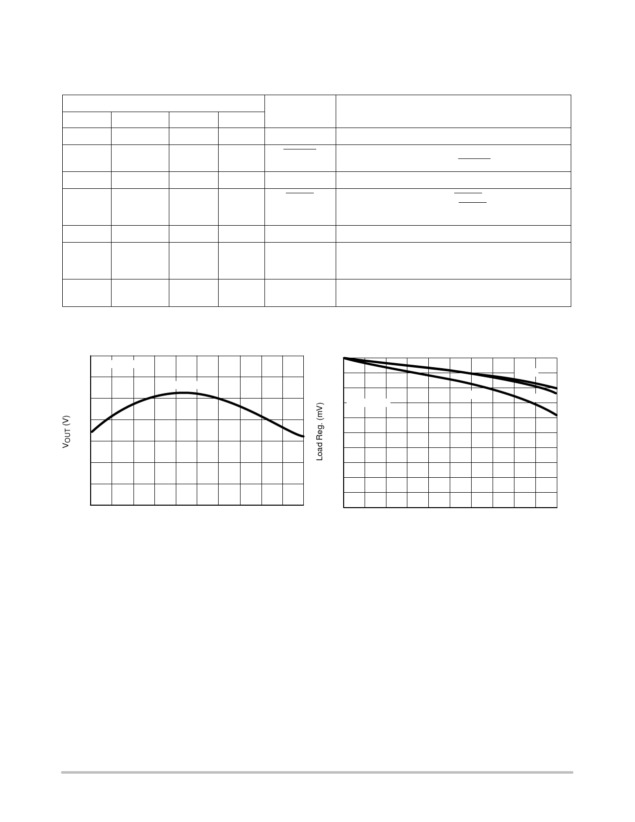
TYPICAL PERFORMANCE CHARACTERISTICS
5.02
5.01
IOUT = 100 mA
5.0
5.0 V @ 25°C
4.99
4.98
4.97
4.96
4.95
−40 −20 0 20 40 60 80 100 120 140 150
Junction Temperature (°C)
Figure 2. Output Voltage vs. Temperature
0
−5
40°C
−10
−15 VIN = 14 V
−20
125°C
25°C
−25
−30
−35
−40
−45
−50
0
100
200
300
400
500
IOUT (mA)
Figure 3. Load Regulation vs. Output
Current Over Temperature
http://onsemi.com
4
Share Link: 