CXB1562AQ 데이터 시트보기 (PDF) - Sony Semiconductor
부품명
상세내역
일치하는 목록
CXB1562AQ Datasheet PDF : 16 Pages
| |||
CXB1562AQ
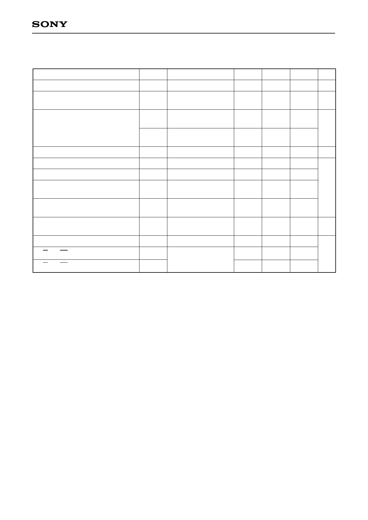
• AC characteristics
(VCC = GND, VEE = –5V±10%, Ta = –40 to +85°C, VCC = VCCD, VCCDA, VCCA VEE = VEED, VEEA)
Item
Maximum input voltage amplitude
Symbol
Conditions
Vmax Single-ended input
Min.
Typ. Max. Unit
1600
mVpp
Amplifier gain
(except for output buffer)
GL
IC internal amplitude
of 400mV
60
dB
Identification maximum voltage
amplitude of alarm level
VminA1
SW pad: Low,
single-ended input
20
VminA2
SW pad: Open High,
single-ended input
50
mVpp
Hysteresis width
SD response assert time
SD response deassert time
∆P
Tas
Tdas
Low → High∗1
High → Low∗2
4
6
7
dB
0
100
2.3
100
SD response assert time for alarm
level default
Tasd
Low → High∗3
0
100
µs
SD response deassert time for alarm
level default
Tdasd
High → Low∗4
2.3
100
Alarm setting level for default
Vdef
UP/DOWN pins; Open,
connect VEEI to VEE.
6.6
8.0
9.3 mV
Propagation delay time
TPD
D to Q
0.95
1.65
2.75
Q/Q SD/SD rise time
Q/Q SD/SD fall time
Tr
RT1 = 50Ω, VT1 = –2 V 0.45
termination
Tf
VEE = –5V, 20% to 80% 0.45
1.6
ns
1.6
∗1 VUP – VDOWN = 100mV, Vin = 100mVpp (single ended), SW pin: High
Peak hold capacitance (CAP2, CAP3 pins) of 470pF; connect VEEI to VEE.
∗2 VUP – VDOWN = 100mV, Vin = 1Vpp (single ended), SW pin: High
Peak hold capacitance (CAP2, CAP3 pins) of 470pF; connect VEEI to VEE.
∗3 Vin = 50mVpp (single ended), SW pin: Low
Peak hold capacitance (CAP2, CAP3 pins) of 470pF; connect VEEI to VEE.
∗4 Vin = 1Vpp (single ended), SW pin: Low
Peak hold capacitance (CAP2, CAP3 pins) of 470pF; connect VEEI to VEE.
–7–
Share Link: 