CXB1562AQ 데이터 시트보기 (PDF) - Sony Semiconductor
부품명
상세내역
일치하는 목록
CXB1562AQ Datasheet PDF : 16 Pages
| |||
CXB1562AQ
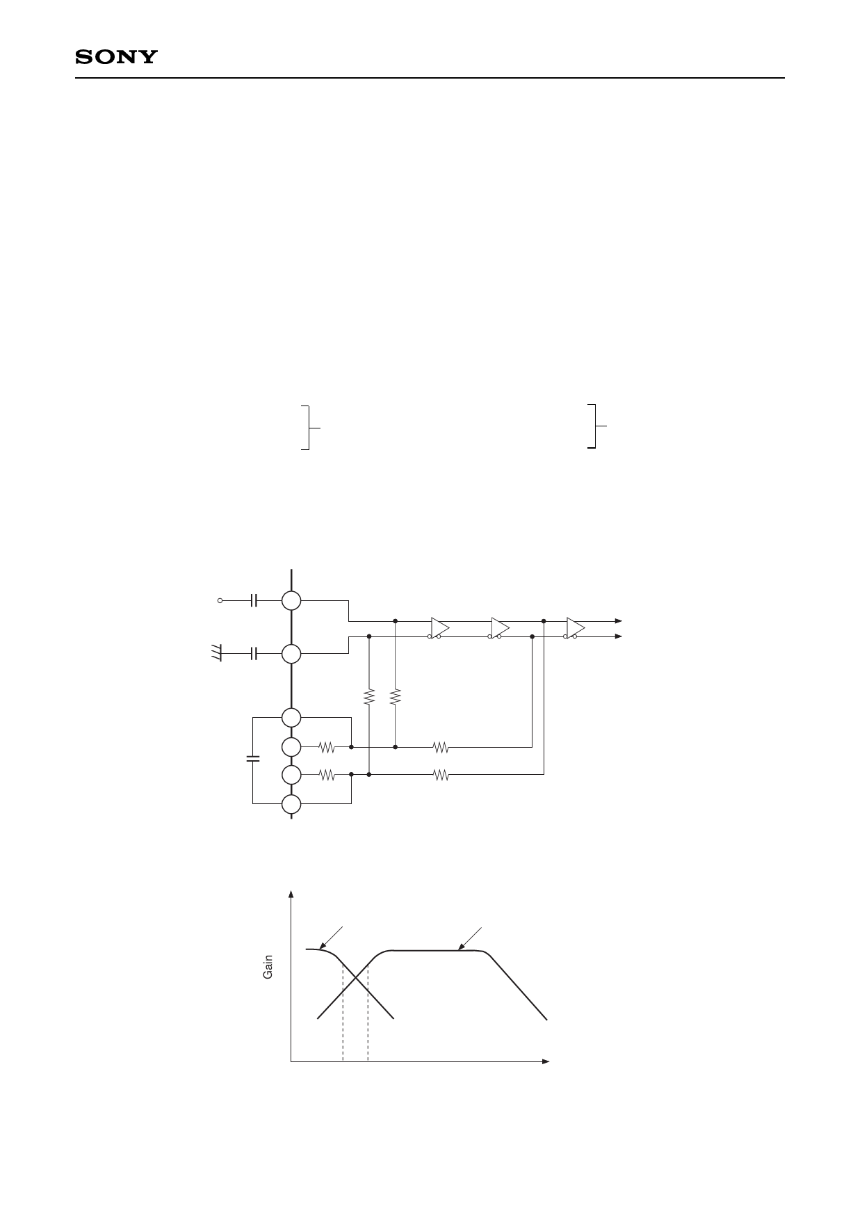
Notes on Operation
1. Limiting amplifier block
The limiting amplifier block is equipped with the auto-offset canceler circuit. When external capacitors C1 and
C2 are connected as shown in Fig. 1, the DC bias is set automatically in this block. External capacitor C1 and
IC internal resistor R1 determine the low input cut-off frequency f2 as shown in Fig. 2. Similarly, external
capacitor C2 and IC internal resistor R2 determine the high cut-off frequency f1 for DC bias feedback. Since
peaking characteristics may occur in the low frequency area of the amplifier gain characteristics depending on
the f1/f2 combination, set the C1 and C2 so as to avoid the occurrence of peaking characteristics. The target
values of R1 and R2 and the typical values of C1 and C2 are as indicated below. When a single-ended input is
used, provide AC grounding by connecting Pin 6 to a capacitor which has the same capacitance as capacitor
C1.
R1 (internal): 1.5kΩ
R2 (internal): 10kΩ
f2: 4.8kHz
f1: 72Hz
C1 (external): 0.022µF
C2 (external): 0.22µF
1kΩ is incorporated between Pins 8 and 9; 2kΩ between Pins 10 and 11. A resistance value which is to be
inserted in parallel with a capacitor f2 can be selected 5 ways (∞, 3kΩ, 2kΩ, 1kΩ, 1k//2kΩ) by external wiring,
and DC feedback can be varied.
D
5
C1
6
C1
8
9
C2
10
11
R1
R3
R4
R1
R2
R2
Fig. 1
To IC interior
Feedback
frequency response
Amplifier
frequency response
f1 f2
Frequency
Fig. 2
– 11 –
Share Link: 