AD6231 데이터 시트보기 (PDF) - Analog Devices
부품명
상세내역
일치하는 목록
AD6231 Datasheet PDF : 10 Pages
| |||
AD8253
Preliminary Technical Data
THEORY OF OPERATION
+VS
+VS
A0
A1
2.2kΩ
+VS
–VS
–VS
2.2kΩ
–IN
A1
10kΩ
10kΩ
–VS
DIGITAL
GAIN
A3
CONTROL
+VS
A2
+IN
2.2kΩ
10kΩ
10kΩ
–VS
+VS
+VS
2.2kΩ
WR
DGND
+VS
OUTPUT
–VS
+VS
REF
–VS
–VS
–VS
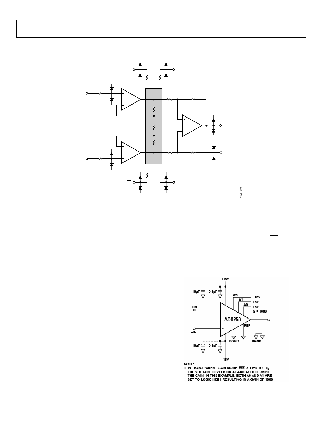
Figure 5. Simplified Schematic
The AD8253 is a monolithic instrumentation amplifier based
on the classic, three op amp topology as shown in Figure 5.
It is fabricated on the Analog Devices, Inc. proprietary iCMOS
process that provides precision, linear performance ,and a robust
digital interface. A parallel interface allows users to digitally
program gains of 1, 10, 100, and 1000. Gain control is achieved
by switching resistors in an internal, precision, resistor array (as
shown in Figure 5). Although the AD8253 has a voltage feed-
back topology, gain bandwidth product increases for gains of 1,
10, and 100 because each gain has its own frequency
compensation. This results in maximum bandwidth at higher
gains.
Transparent Gain Mode
The easiest way to set the gain is to program it directly via a
logic high or logic low voltage applied to A0 and A1. Figure 6
shows an example of this gain setting method, referred to through-
out the data sheet as transparent gain mode. Tie WR to the
negative supply to engage transparent gain mode. In this mode,
any change in voltage applied to A0 and A1 from logic low to
logic high, or vice versa, immediately results in a gain change.
Table 5 is the truth table for transparent gain mode and Figure 6
shows the AD8253 configured in transparent gain mode.
All internal amplifiers employ distortion cancellation circuitry
and achieve high linearity and ultralow THD. Laser trimmed
resistors allow for a maximum gain error of less than 0.03% for
G = 1, and minimum CMRR of 120 dB for G = 1000. A pinout
optimized for high CMRR over frequency enables the AD8253
to offer CMRR over frequency of 80 dB at 50 kHz (G = 1). The
balanced input reduces the parasitics that, in the past, had
adversely affected CMRR performance.
GAIN SELECTION
This section shows users how to configure the AD8253 for basic
operation. Logic low and Logic high voltage limits are listed in
the Specifications section. Typically, logic low is 0 V and
logic high is 5 V; both voltages are measured with respect
to DGND. Refer to the specifications table (Table 2) for
the permissible voltage range of DGND. The gain of the
AD8253 can be set using two methods.
Figure 6. Transparent Gain Mode, A0 and A1 = High, G = 1000
Rev. prA | Page 8 of 10
Share Link: 