AD7641ASTRL 데이터 시트보기 (PDF) - Analog Devices
부품명
상세내역
일치하는 목록
AD7641ASTRL Datasheet PDF : 28 Pages
| |||
AD7641
TYPICAL CONNECTION DIAGRAM
Figure 23 shows a typical connection diagram for the AD7641.
Different circuitry shown in this diagram is optional and is
discussed in the following sections.
ANALOG INPUTS
Figure 24 shows an equivalent circuit of the input structure of
the AD7641.
The two diodes, D1 and D2, provide ESD protection for the
analog inputs IN+ and IN−. Care must be taken to ensure that
the analog input signal never exceeds the supply rails by more
than 0.3 V, because this causes the diodes to become forward-
biased and start conducting current. These diodes can handle a
forward-biased current of 100 mA maximum. For instance,
these conditions could eventually occur when the input buffer’s
U1 or U2 supplies are different from AVDD. In such a case, an
input buffer with a short-circuit current limitation can be used
to protect the part.
AVDD
D1
IN+ OR IN–
CPIN
D2
AGND
RIN
CIN
Figure 24. AD7641 Simplified Analog Input
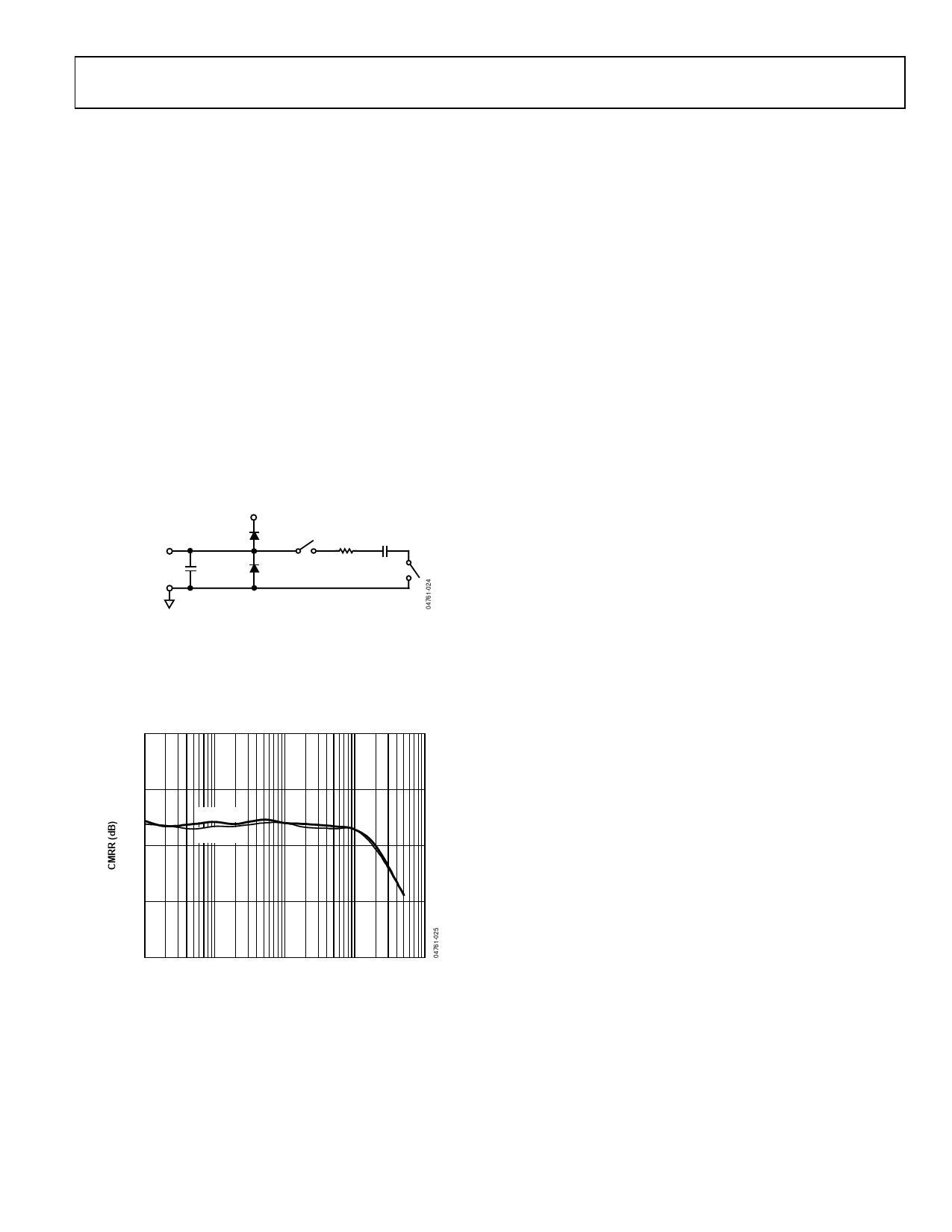
The analog input of the AD7641 is a true differential structure.
By using this differential input, small signals common to both
inputs are rejected, as shown in Figure 25, representing the
typical CMRR over frequency with internal and external references.
65
60
EXT REF
INT REF
55
50
45
1
10
100
1000
FREQUENCY (kHz)
Figure 25. Analog Input CMRR vs. Frequency
10000
During the acquisition phase for ac signals, the impedance of
the analog inputs, IN+ and IN−, can be modeled as a parallel
combination of capacitor CPIN and the network formed by the
series connection of RIN and CIN. CPIN is primarily the pin
capacitance. RIN is typically 175 Ω and is a lumped component
comprised of some serial resistors and the on resistance of the
switches. CIN is typically 12 pF and is mainly the ADC sampling
capacitor. During the conversion phase, when the switches are
opened, the input impedance is limited to CPIN. RIN and CIN
make a 1-pole, low-pass filter that has a typical −3 dB cutoff
frequency of 50 MHz, thereby reducing an undesirable aliasing
effect and limiting the noise coming from the inputs.
Because the input impedance of the AD7641 is very high, the
AD7641 can be directly driven by a low impedance source
without gain error. To further improve the noise filtering achieved
by the AD7641 analog input circuit, an external 1-pole RC filter
between the amplifier’s outputs and the ADC analog inputs can
be used, as shown in Figure 23. However, large source impedances
significantly affect the ac performance, especially the total
harmonic distortion (THD). The maximum source impedance
depends on the amount of THD that can be tolerated. The THD
degrades as a function of the source impedance and the maximum
input frequency.
MULTIPLEXED INPUTS
When using the full 2 MSPS throughput in multiplexed
applications for a full-scale step, the RC filter, as shown in
Figure 23, does not settle in the required acquisition time, t8.
These values are chosen to optimize the best SNR perform-ance
of the AD7641. To use the full 2 MSPS throughput in
multiplexed applicaitons, the RC should be adjusted to satisfy t8
(which is ~ 8.5 × RC time constant). However, lowering R and C
increases the RC filter bandwidth and allows more noise into the
AD7641, which degrades SNR. To preserve the SNR performance
in these applications using the RC filter shown in Figure 23,
the AD7641 should be run with t8 > 350 ns; or approximately
1/(t7 + t8) ~ 1.35 MSPS in wideband and warp modes.
DRIVER AMPLIFIER CHOICE
Although the AD7641 is easy to drive, the driver amplifier
needs to meet the following requirements:
• For multichannel, multiplexed applications, the driver
amplifier and the AD7641 analog input circuit must be
able to settle for a full-scale step of the capacitor array at an
18-bit level (0.0004%). In the amplifier’s data sheet, settling
at 0.1% to 0.01% is more commonly specified. This could
differ significantly from the settling time at a 18-bit level
and should be verified prior to driver selection. The
AD8021 op amp, which combines ultralow noise and high
gain bandwidth, meets this settling time requirement even
when used with gains up to 13.
Rev. 0 | Page 17 of 28
Share Link: 