AD7631(2011) 데이터 시트보기 (PDF) - Analog Devices
부품명
상세내역
일치하는 목록
AD7631 Datasheet PDF : 32 Pages
| |||
AD7631
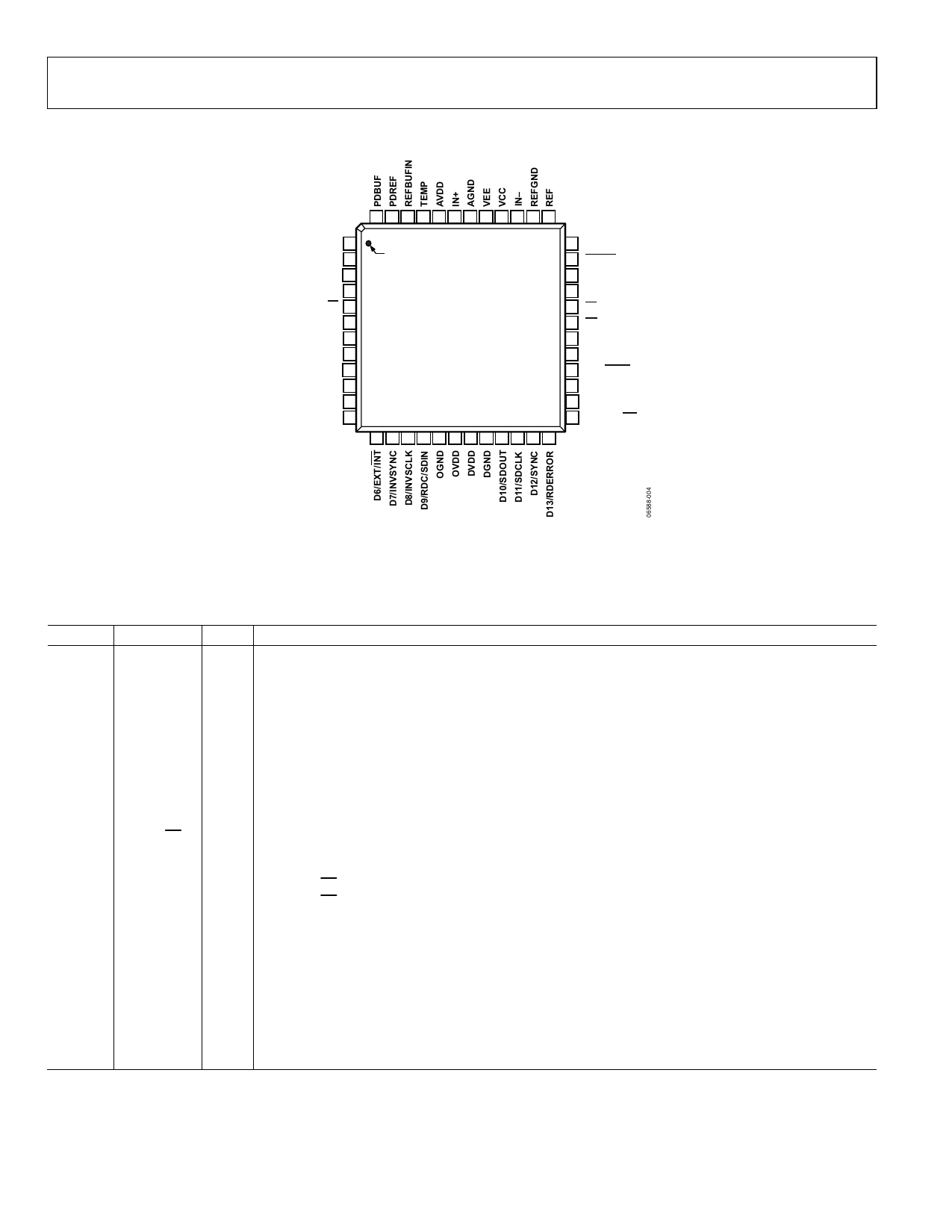
PIN CONFIGURATION AND FUNCTION DESCRIPTIONS
48 47 46 45 44 43 42 41 40 39 38 37
AGND 1
AVDD 2
MODE0 3
MODE1 4
D0/OB/2C 5
OGND 6
OGND 7
D1/A0 8
D2/A1 9
D3 10
D4/DIVSCLK[0] 11
D5/DIVSCLK[1] 12
PIN 1
AD7631
TOP VIEW
(Not to Scale)
36 BIPOLAR
35 CNVST
34 PD
33 RESET
32 CS
31 RD
30 TEN
29 BUSY
28 D17/SCCS
27 D16/SCCLK
26 D15/SCIN
25 D14/HW/SW
13 14 15 16 17 18 19 20 21 22 23 24
NOTES
1. FOR THE LEAD FRAME CHIP SCALE PACKAGE (LFCSP), THE EXPOSED PAD
SHOULD BE CONNECTED TO VEE. THIS CONNECTION IS NOT REQUIRED TO
MEET THE ELECTRICAL PERFORMANCES.
Figure 4. Pin Configuration
Table 6. Pin Function Descriptions
Pin No. Mnemonic Type1 Description
1, 42
AGND
P
Analog Power Ground Pins. Ground reference point for all analog I/O. All analog I/O should be
referenced to AGND and should be connected to the analog ground plane of the system. In addition,
the AGND, DGND, and OGND voltages should be at the same potential.
2, 44
AVDD
P
Analog Power Pins. Nominally 4.75 V to 5.25 V and decoupled with 10 μF and 100 nF capacitors.
3, 4
MODE[0:1] DI
Data Input/Output Interface Mode Selection.
Interface Mode
MODE1 MODE0 Description
0
Low
Low
18-bit interface
1
Low
High
16-bit interface
2
High
Low
8-bit (byte) interface
3
High
High
Serial interface
5
D0/OB/2C DI/O2 In 18-bit parallel mode, this output is used as Bit 0 of the parallel port data output bus, and the data
coding is straight binary. In all other modes, this pin allows the choice of straight binary or twos
complement.
When OB/2C = high, the digital output is straight binary.
When OB/2C = low, the MSB is inverted resulting in a twos complement output from its internal
shift register.
6, 7, 17 OGND
P
Input/Output Interface Digital Power Ground. Ground reference point for digital outputs. Should
be connected to the system digital ground ideally at the same potential as AGND and DGND.
8
D1/A0
DI/O When MODE[1:0] = 0, this pin is Bit 1 of the parallel port data output bus. In all other modes, this
input pin controls the form in which data is output as shown in Table 7.
9
D2/A1
DI/O When MODE[1:0] = 0, this pin is Bit 2 of the parallel port data output bus.
When MODE[1:0] = 1 or 2, this input pin controls the form in which data is output as shown in Table 7.
10
D3
DO When MODE[1:0] = 0, 1, or 2, this output is used as Bit 3 of the parallel port data output bus.
This pin is always an output, regardless of the interface mode.
Rev. A | Page 8 of 32
Share Link: 