74LVQ299 데이터 시트보기 (PDF) - STMicroelectronics
부품명
상세내역
일치하는 목록
74LVQ299 Datasheet PDF : 12 Pages
| |||
74LVQ299
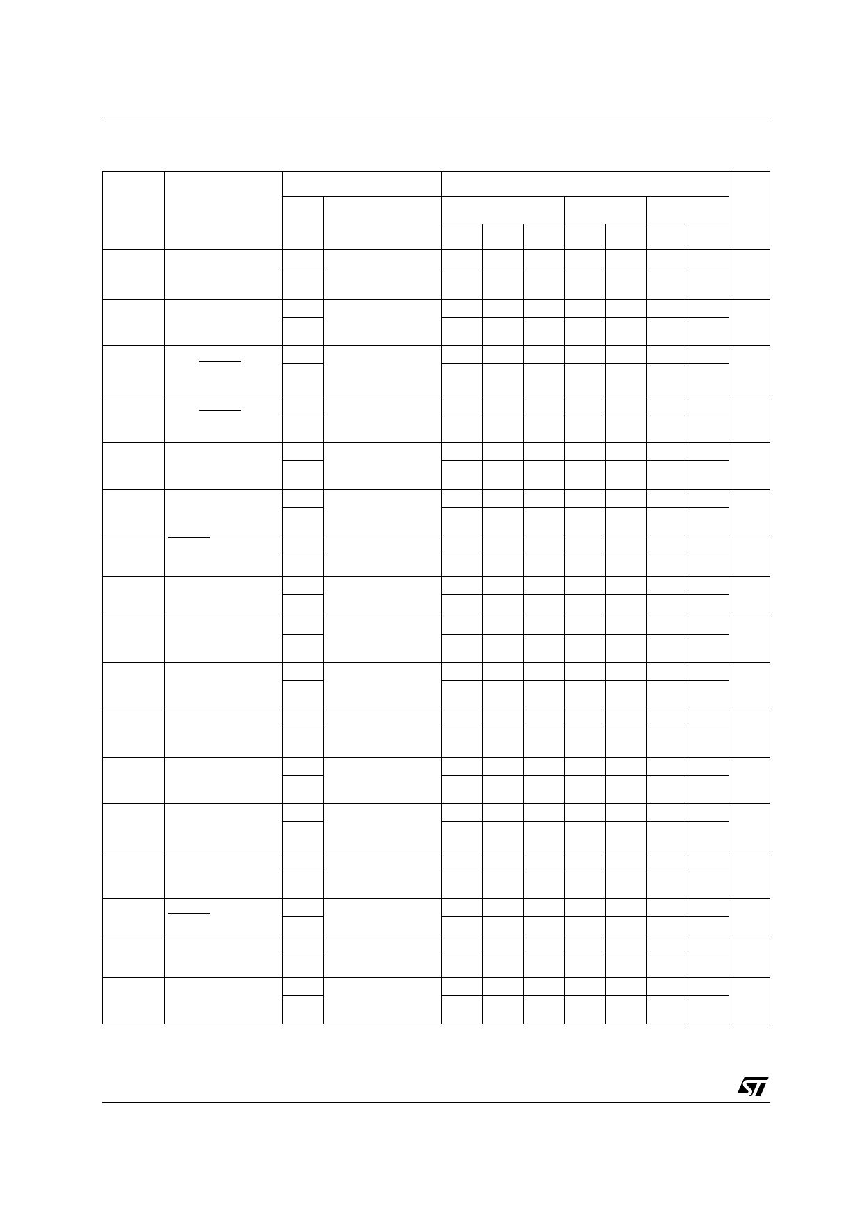
AC ELECTRICAL CHARACTERISTICS(CL = 50 pF, RL = 500 Ω, Input tr = tf = 3ns)
Test Condition
Value
Symbol
Parameter
VCC
(V)
TA = 25°C
-40 to 85°C -55 to 125°C Unit
Min. Typ. Max. Min. Max. Min. Max.
tPLH tPHL Propagation Delay
Time CLOCK to
Q’A or Q’H
2.7
3.3(*)
9.7 15.0
8.2 12.0
17.5
14.0
20.0
ns
16.5
tPLH tPHL Propagation Delay
Time CLOCK to
A/QA, H/QH
2.7
3.3(*)
9.8 15.0
8.3 12.0
17.5
14.0
20.0
ns
16.5
tPHL Propagation Delay 2.7
Time CLEAR to
Q’A or Q’H
3.3(*)
8.4 14.0
7.1 11.0
16.5
13.0
19.0
ns
15.0
tPHL Propagation Delay 2.7
Time CLEAR to
A/QA, H/QH
3.3(*)
8.9 15.0
7.4 12.0
17.5
14.0
20.0
ns
16.5
tPZL tPZH Output Enable
Time G1 or G2 to
A/QA, H/QH
2.7
3.3(*)
9.9 15.0
8.0 12.0
17.5
14.0
20.0
ns
16.5
tPLZ tPHZ Output Disable
Time G1 or G2 to
A/QA, H/QH
2.7
3.3(*)
9.8 15.0
8.0 12.0
17.5
14.0
20.0
ns
16.5
tW CLEAR Pulse
Width LOW
2.7
3.3(*)
5.0 2.1
5.0
5.0
ns
4.0 2.0
4.0
4.0
tW CLOCK Pulse
Width LOW
2.7
3.3(*)
5.0 2.1
5.0
5.0
ns
4.0 2.0
4.0
4.0
ts
Setup Time HIGH 2.7
or LOW (A/QA, H/
QH to CLOCK)
3.3(*)
4.0 1.4
4.0
4.0
ns
3.0 1.1
3.0
3.0
th Hold Time HIGH or 2.7
LOW (A/QA, H/QH
to CLOCK)
3.3(*)
1.0 -1.3
1.0
1.0
ns
1.0 -1.0
1.0
1.0
ts
Setup Time HIGH 2.7
or LOW (S0 or S1
to CLOCK)
3.3(*)
6.0 3.1
6.0
6.0
ns
5.0 2.5
5.0
5.0
th Hold Time HIGH or 2.7
LOW (S0 or S1 to
CLOCK)
3.3(*)
1.0 -3.1
1.0
1.0
ns
1.0 -2.6
1.0
1.0
ts
Setup Time HIGH 2.7
or LOW (SR or SL
to CLOCK)
3.3(*)
4.0 1.5
4.0
4.0
ns
3.0 1.1
3.0
3.0
th Hold Time HIGH or 2.7
LOW (SR or SL to
CLOCK)
3.3(*)
1.0 -1.5
1.0
1.0
ns
1.0 -1.1
1.0
1.0
tREM
Recovery Time
2.7
CLEAR to CLOCK 3.3(*)
1.0 -0.7
1.0
1.0
ns
1.0 -0.5
1.0
1.0
fMAX Maximum Clock
Frequency
2.7
3.3(*)
100 150
80
60
ns
120 180
100
80
tOSLH
tOSHL
Output To Output
Skew Time
(note1, 2)
2.7
3.3(*)
0.5 1.0
1.0
1.0
0.5 1.0
1.0
1.0 ns
1) Skew is defined as the absolute value of the difference between the actual propagation delay for any two outputs of the same device switch-
ing in the same direction, either HIGH or LOW (tOSLH = |tPLHm - tPLHn|, tOSHL = |tPHLm - tPHLn|)
2) Parameter guaranteed by design
(*) Voltage range is 3.3V ± 0.3V
6/12
Share Link: 