74LVQ299 데이터 시트보기 (PDF) - STMicroelectronics
부품명
상세내역
일치하는 목록
74LVQ299 Datasheet PDF : 12 Pages
| |||
74LVQ299
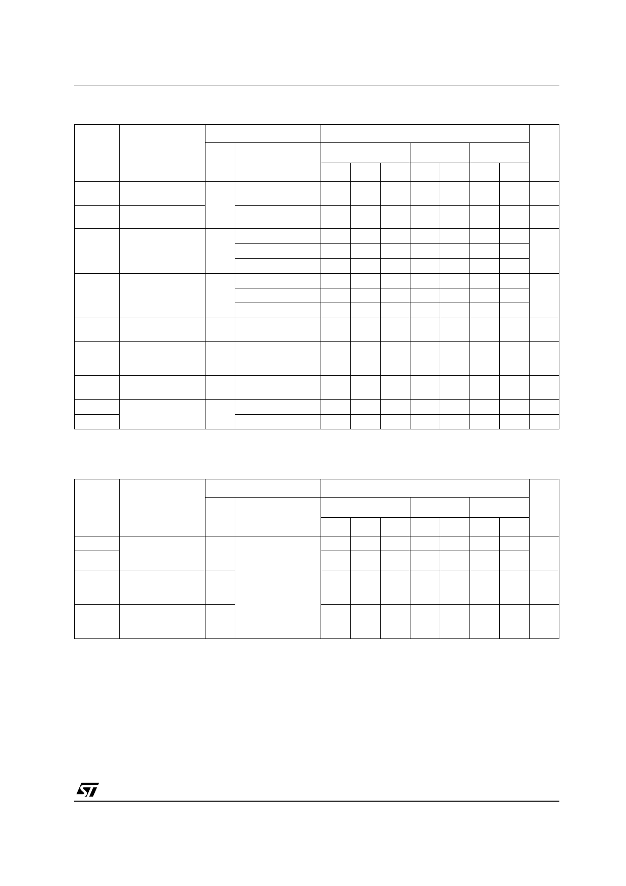
DC SPECIFICATIONS
Test Condition
Value
Symbol
Parameter
VCC
(V)
TA = 25°C
-40 to 85°C -55 to 125°C Unit
Min. Typ. Max. Min. Max. Min. Max.
VIH High Level Input
Voltage
3.0 to
VIL Low Level Input
3.6
Voltage
2.0
2.0
2.0
V
0.8
0.8
0.8 V
VOH High Level Output
IO=-50 µA
2.9 2.99
2.9
2.9
Voltage
3.0
IO=-12 mA
2.58
2.48
2.48
V
IO=-24 mA
2.2
2.2
VOL Low Level Output
Voltage
3.0
IO=50 µA
IO=12 mA
0.002 0.1
0 0.36
0.1
0.44
0.1
0.44 V
IO=24 mA
0.55
0.55
II
Input Leakage
Current
3.6 VI = VCC or GND
± 0.1
±1
± 1 µA
IOZ High Impedance
Output Leakage
Current
3.6
VI = VIH or VIL
VO = VCC or GND
±0.25
± 2.5
± 5.0 µA
ICC
Quiescent Supply
Current
3.6 VI = VCC or GND
4
40
40 µA
IOLD
IOHD
Dynamic Output
Current (note 1, 2)
3.6 VOLD = 0.8 V max
VOHD = 2 V min
36
25
mA
-25
-25
mA
1) Maximum test duration 2ms, one output loaded at time
2) Incident wave switching is guaranteed on transmission lines with impedances as low as 75Ω
DYNAMIC SWITCHING CHARACTERISTICS
Test Condition
Value
Symbol
Parameter
VCC
(V)
TA = 25°C
-40 to 85°C -55 to 125°C Unit
Min. Typ. Max. Min. Max. Min. Max.
VOLP Dynamic Low
0.5 0.8
Voltage Quiet
3.3
V
VOLV Output (note 1, 2)
-0.8 -0.6
VIHD Dynamic High
3.3
2
V
Voltage Input
CL = 50 pF
(note 1, 3)
VILD Dynamic Low
3.3
Voltage Input
(note 1, 3)
0.8
V
1) Worst case package.
2) Max number of outputs defined as (n). Data inputs are driven 0V to 3.3V, (n-1) outputs switching and one output at GND.
3) Max number of data inputs (n) switching. (n-1) switching 0V to 3.3V. Inputs under test switching: 3.3V to threshold (VILD), 0V to threshold
(VIHD), f=1MHz.
5/12
Share Link: 