74F598 데이터 시트보기 (PDF) - Philips Electronics
부품명
상세내역
일치하는 목록
74F598 Datasheet PDF : 14 Pages
| |||
Philips Semiconductors
8-bit shift register with input storage registers (3-State)
Product specification
74F598
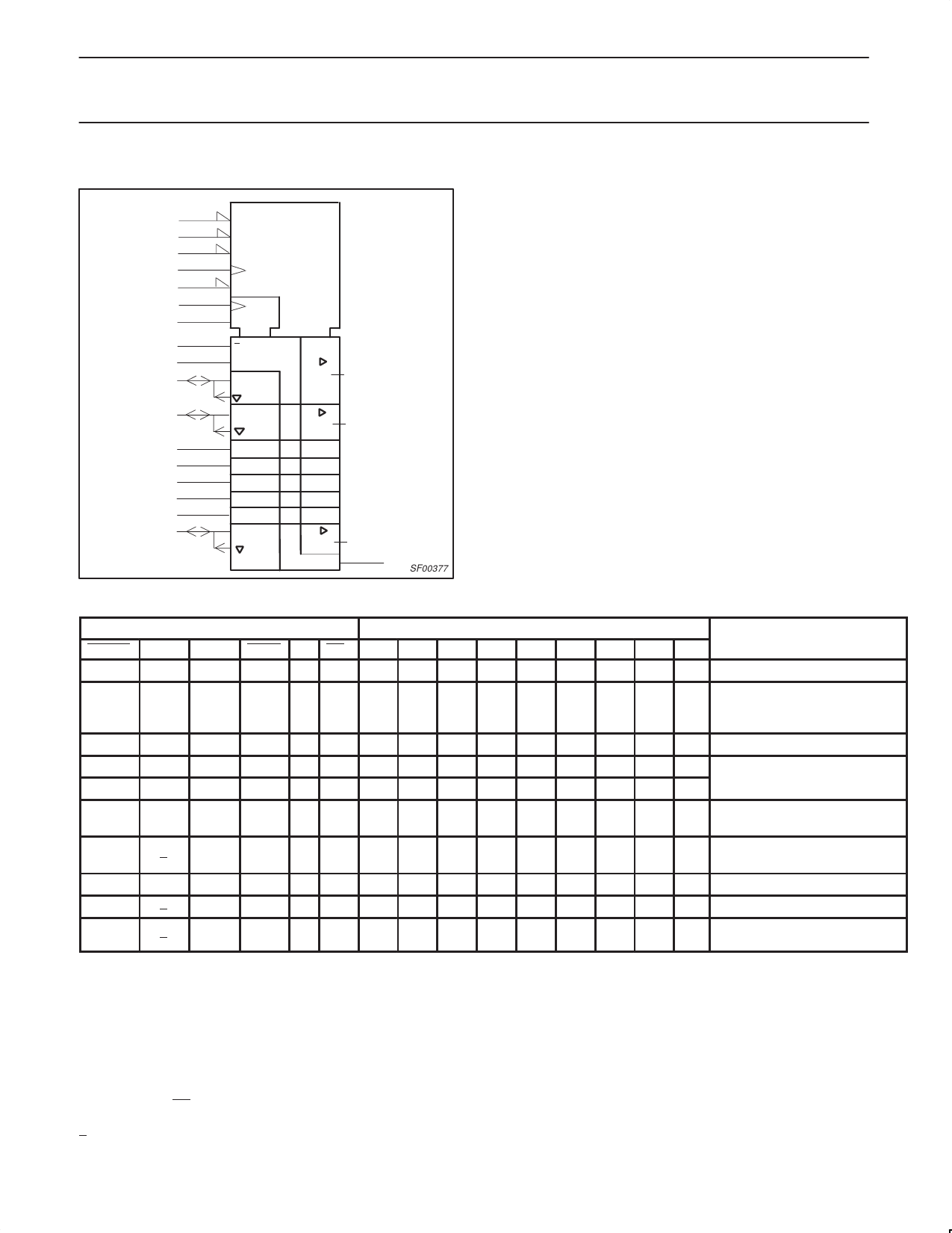
IEC/IEEE SYMBOL
16
SRG8
EN14
12
R
14
G4
13
4C5/4→
9
C2
15
C1
19
G1
18
1, 5D
17
1, 5D
1
2D
Z6
3D
6, 14
2
2D
7, 14 3D Z7
3
4
5
6
7
8
2D
13, 14 3D Z13
11
SF00377
FUNCTION TABLE
INPUTS
INPUTS/OUTPUTS
SHRST STCP SHCP SHLD S OE* I/O0 I/O1 I/O2 I/O3 I/O4 I/O5 I/O6 I/O7 Q7
OPERATING MODE
L
X
L
H XL
L
L
L
L
L
L
L
L L Clear shift register
L
X
L
L XL
Invalid, state of shift register in-
determinate when signal is re-
moved
X
↑
X
X X H I0 I1 I2 I3 I4 I5 I6 I7 O7 Load data to storage register
H
X
↑
H L L Ds0 O0 O1 O2 O3 O4 O5 O6 O6 Shift right
H
X
↑
H H L Ds1 O0 O1 O2 O3 O4 O5 O6 O6
H
↑
L
L
XH
I0 I1
I2 I3
I4 I5 I6
I7
O7
Load data directly to shift regis-
ter
H
↑
L
L
X
X
O0
O1
O2
O3
O4
O5
O6
O7
O7
Data transferred from storage
register to shift register
X
X
X
X
XH
Z
Z
Z
Z
Z
Z
Z
Z NC 3–State
H
↑
X
H X X NC NC NC NC NC NC NC NC NC Hold
H
↑
H
X
X
X
NC
NC
NC
NC
NC
NC
NC
NC
NC
Hold (no storage or shift register
load
Notes to function table
D0 – D7 = The level of the steady state inputs to the serial multiplexer.
H = High voltage level
I0 – I7 = The level of the steady state input at the respective I/O terminal is loaded into the flip–flop while the flip–flop outputs ( except Q7) are isolated
from the I/O terminal.
L = Low voltage level
NC= No change
O0 – O7 = The level of the respective Qn flip–flop prior to the last clock Low–to–High transition
X = Don’t care
Z = High impedance ”off” state
* = When the OE input is High, all I/O terminals are at the High impedance state, sequential operation or cleaning of the register is not affected.
↑ = Low–to–High clock transition
↑ = Not Low–to–High clock transition
1991 Oct 21
3
Share Link: 