4-5435166-9(RevB) 데이터 시트보기 (PDF) - Tyco Electronics
부품명
상세내역
일치하는 목록
4-5435166-9 Datasheet PDF : 7 Pages
| |||
DIP Programming Switches (7000 and 7100 Series)
114-1056
NOTE
Where the above environmental conditions exist, phosphor-bronze contacts are recommended if available.
3.4. Printed Circuit (PC) Board Requirements
A. Material and Thickness
The pc board material must be glass epoxy (FR–4 or G–10). The pc board thickness shall be 2.36 mm
[.093 in.].
NOTE
Contact the Product Information Center at the number listed at the bottom of page 1 for suitability of other board
materials and thicknesses.
B. Tolerance
Maximum allowable bow of the pc board must be 0.08 mm [.003 in.] over each 25.4 mm [1.000 in.] of
length.
C. PC Board Layout
The solder tail contact holes in the pc board must be precisely located to ensure proper placement and
optimum performance of the switch. The pc board layout dimensions and tolerances shown in Figure 2
must be observed when preparing pc boards for the various switches. The layout shows the top
(component) side of the board.
2.54 + 0.13
[.100 + .005]
Typ
0.89 + 0.13
[.035 + .005]
Dia Typ
7.62 + 0.13
[.300 + .005]
Figure 2
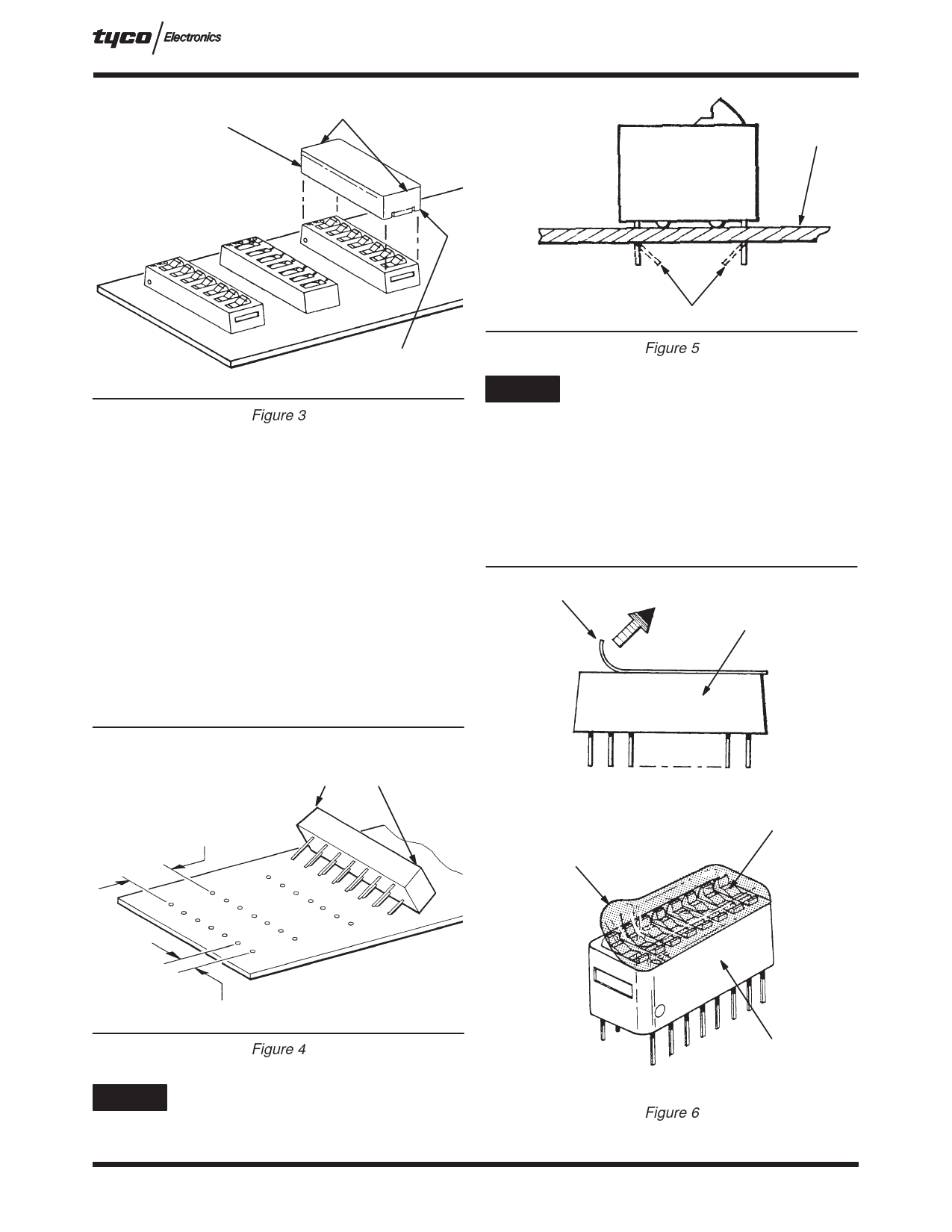
3.5. PC Board Solder Tail Holes
The holes in the pc board for the solder tails must be drilled and plated through to specific dimensions. See
Figure 3.
Board Thickness
2.36 [.093]
ÉÉÏÉÏÉ (Nominal)
ÉÉÉÉÉÉÉÉÏÏÏÏÌÌÌÌÉÉÉÉÏÏÏÏÉÉÉÉ Tin/Lead Thickness
(As Required)
Dia of Finished Hole After Plating
∅0.89 +0.13 [.035 +.005]
Drilled Hole Diameter
(As Required)
ÉÉÉÉÉÉÏÏÏÏÏÌÌÌÌÌÉÉÉÉÉÉÉÉÉÉÉÉ
Pad Diameter
(As Required)
Copper Thickness (As Required)
(Maximum Hardness of Copper to
be 150 Knoop)
Figure 3
Rev B
3 of 7
Share Link: 