EN29F002(2000) 데이터 시트보기 (PDF) - Eon Silicon Solution Inc.
부품명
상세내역
일치하는 목록
EN29F002 Datasheet PDF : 32 Pages
| |||
EN29F002 / EN29F002N
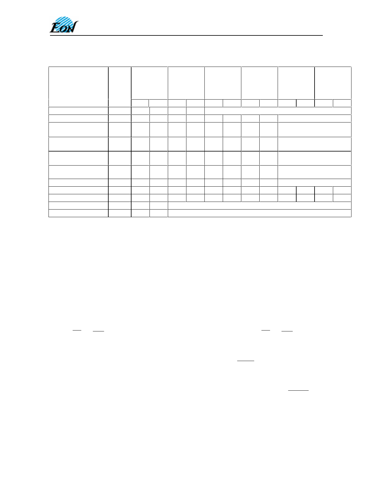
Table 5. EN29F002 Command Definitions
Command
Sequence
Read/Reset
Read/Reset
Read/Reset
AutoSelect
Manufacturer ID
AutoSelect Device ID
(Top Boot)
AutoSelect Device ID
(Bottom Boot)
AutoSelect Block
Protect Verify
Byte Program
Chip Erase
Block Erase
Block Erase Suspend
Block Erase Resume
Write
Cycles
Req’d
1
4
4
4
4
4
4
6
6
1
1
1st
Write Cycle
2nd
Write Cycle
3rd
Write Cycle
4th
Write Cycle
5th
Write Cycle
6th
Write Cycle
Addr Data
XXXh F0h
555h AAh
555h AAh
555h AAh
555h AAh
555h AAh
555h AAh
555h AAh
555h AAh
xxxh B0h
xxxh 30h
Addr Data
RA RD
AAAh 55h
AAAh 55h
AAAh 55h
AAAh 55h
AAAh 55h
AAAh 55h
AAAh 55h
AAAh 55h
Addr Data
555h F0h
555h 90h
555h 90h
555h 90h
555h 90h
555h A0h
555h 80h
555h 80h
Addr Data
RA
000h/
100h
001h/
101h
001h/
101h
BA &
02h
PA
555h
555h
RD
7Fh/
1Ch
7Fh/
92h
7Fh/
97h
00h/
01h
PD
AAh
AAh
Addr Data
AAAh 55h
AAAh 55h
Addr Data
555h 10h
BA 30h
Notes:
RA = Read Address: address of the memory location to be read
RD = Read Data: data read from location RA during Read operation
PA = Program Address: address of the memory location to be programmed
PD = Program Data: data to be programmed at location PA
BA = Block Address: address of the block to be erased. Address bits A17-A13 uniquely select any block.
Byte Programming Command
Programming the EN29F002 is performed on a byte-by-byte basis using a four bus-cycle operation
(two unlock write cycles followed by the Program Setup command and Program Data Write cycle).
When the program command is executed, no additional CPU controls or timings are necessary. The
program operation is terminated automatically by an internal timer. Address is latched on the falling
edge of CE or W E , whichever is last; data is latched on the rising edge of CE or W E , whichever is
first. The program operation is completed when EN29F002 returns the equivalent data to the
programmed location.
Programming status may be checked by sampling data on DQ7 (DATA polling) or on DQ6 (toggle
bit). Changing data from 0 to 1 requires an erase operation. When programming time limit is
exceeded, DQ5 will produce a logical “1” and a Reset command can return the device to Read mode.
EN29F002 ignores commands written during Byte Programming. If a hardware RESET occurs
during Byte Programming, data at the programmed location may get corrupted. Programming is
allowed in any sequence and across any block boundary.
Chip Erase Command
An auto Chip Erase algorithm is employed when the Chip Erase command sequence is performed.
Although the Chip Erase command requires six bus cycles: two unlock write cycles, a setup
command, two additional unlock write cycles and the chip erase command, the user is responsible
for writing only the Erase Setup command and the Erase command. The Erase Setup command is
4800 Great America Parkway, Suite 202
8
Santa Clara, CA 95054
Tel: 408-235-8680
Fax: 408-235-8685
Share Link: 