NCP600 데이터 시트보기 (PDF) - ON Semiconductor
부품명
상세내역
일치하는 목록
NCP600 Datasheet PDF : 15 Pages
| |||
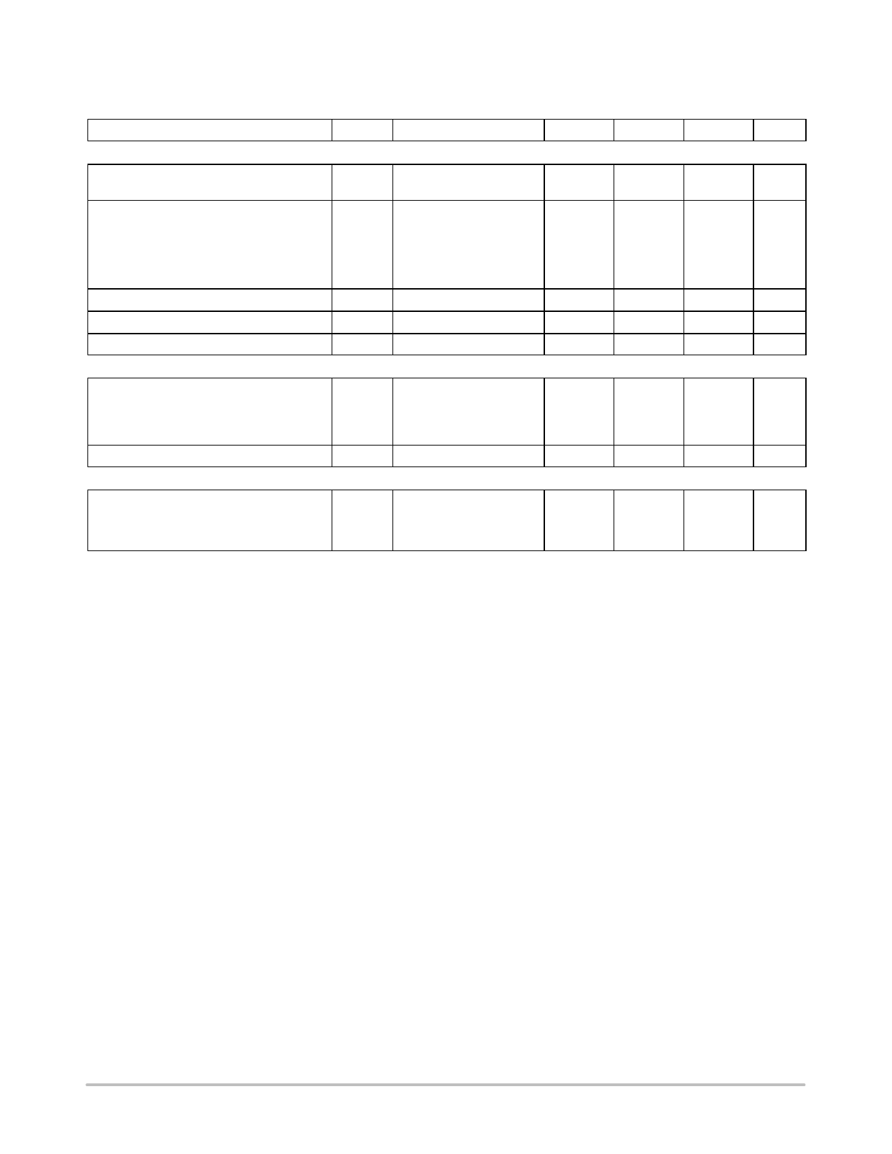
NCP600
ELECTRICAL CHARACTERISTICS (Vin = Vout + 0.5 V, For Typical Values TA = 25°C, For Min/Max Values TA = −40°C to
125°C, unless otherwise specified.) (Note 10)
Characteristic
Symbol
Test Conditions
Min
Typ
Max
Unit
General
Disable Current
Ground Current
1.25 V (Adjustable)
1.3 V
1.5 V
1.8 V to 3.0 V
3.3 V to 5.0 V
IDIS
ENABLE = 0 V, Vin = 6 V
−
TA = −40°C to 85°C
IGND ENABLE = 0.9 V,
Iout = 1.0 mA to 150 mA
−
−
−
−
−
0.01
1.0
mA
mA
100
135
135
150
135
170
140
175
145
180
Thermal Shutdown Temperature (Note 11)
TSD
Thermal Shutdown Hysteresis (Note 11)
TSH
ADJ Input Bias Current
IADJ
Chip Enable
−
175
−
10
−0.75
−
−
°C
−
°C
0.75
mA
ENABLE Input Threshold Voltage
Voltage Increasing, Logic High
Vth(EN)
0.9
−
V
−
Voltage Decreasing, Logic Low
−
−
0.4
Enable Input Bias Current (Note 11)
IEN
Timing
−
3.0
100
nA
Output Turn On Time (Note 11)
1.25 V
1.3 V to 3.5 V
5.0 V
tEN
ENABLE = 0 V to Vin
ms
−
15
25
−
15
25
−
30
50
10. Performance guaranteed over the indicated operating temperature range by design and/or characterization, production tested at
TJ = TA = 25°C. Low duty cycle pulse techniques are used during testing to maintain the junction temperature as close to ambient as possible.
11. Values based on design and/or characterization.
http://onsemi.com
4
Share Link: 