NCP600 데이터 시트보기 (PDF) - ON Semiconductor
부품명
상세내역
일치하는 목록
NCP600 Datasheet PDF : 15 Pages
| |||
NCP600
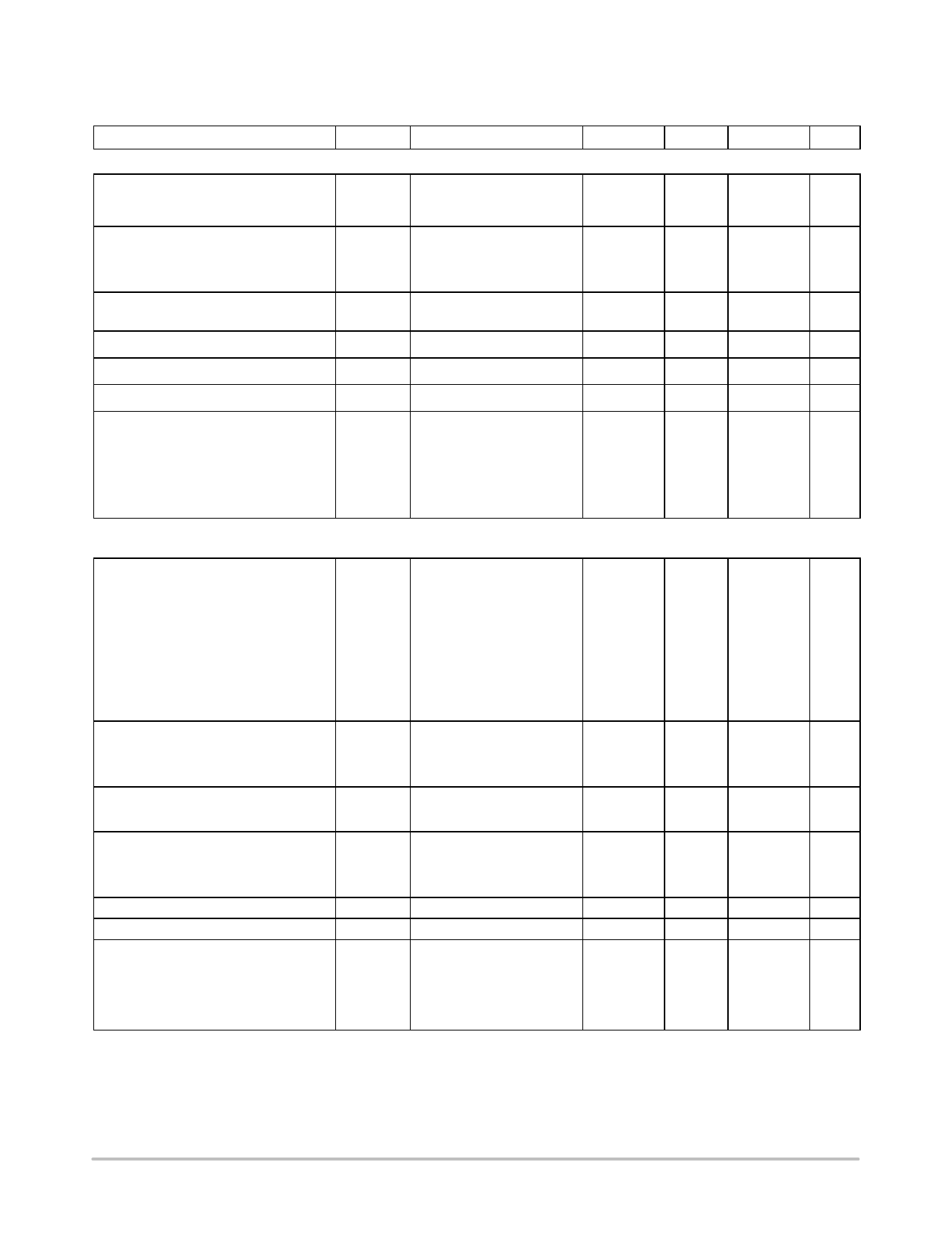
ELECTRICAL CHARACTERISTICS (Vin = 1.750 V, Vout = 1.250 V, Cin = Cout =1.0 mF, for typical values TA = 25°C, for min/max
values TA = −40°C to 125°C, unless otherwise specified.) (Note 8)
Characteristic
Symbol
Test Conditions
Min
Typ
Max
Unit
Regulator Output (Adjustable Voltage Version)
Output Voltage
Power Supply Ripple Rejection
(Vin = Vout + 1.0 V + 0.5 Vp−p)
Vout
PSRR
Iout = 1.0 mA to 150 mA
Vin = 1.75 V to 6.0 V,
Vout = ADJ
Iout = 1.0 mA to 150 mA
f = 120 Hz
f = 1.0 kHz
f = 10 kHz
1.231
1.250
1.269
V
(−1.5%)
(+1.5%)
dB
−
62
−
−
55
−
−
38
−
Line Regulation
Load Regulation
Output Noise Voltage (Note 9)
Output Short Circuit Current
Dropout Voltage
1.25 V
1.3 V
1.5 V
1.8 V
2.5 V
2.8 V to 5.0 V
Regline
Vin = 1.750 V to 6.0 V,
Iout = 1.0 mA
−
1.0
10
mV
Regload Iout = 1.0 mA to 150 mA
−
2.0
15
mV
Vn
f = 10 Hz to 100 kHz
−
50
−
mVrms
Isc
Vout = 0 V
300
550
800
mA
VDO
Measured at: Vout – 2.0%,
mV
Iout = 150 mA
−
175
250
−
175
250
−
150
225
−
125
175
−
100
150
−
75
125
Regulator Output (Fixed Voltage Version) (Vin = Vout + 0.5 V, Cin = Cout =1.0 mF, for typical values TA = 25°C, for min/max values TA =
−40°C to 125°C; unless otherwise noted.) (Notes 8)
Output Voltage
1.3 V
1.5 V
1.8 V
2.5 V
2.8 V
3.0 V
3.3 V
3.5 V
5.0 V
Vout
Iout = 1.0 mA to 150 mA
Vin = (Vout + 0.5 V) to 6.0 V
1.274
1.470
1.764
2.450
2.744
2.940
3.234
3.430
4.900
(−2%)
V
1.326
1.530
1.836
2.550
2.856
3.060
3.366
3.570
5.100
(+2%)
Power Supply Ripple Rejection (Note 9)
(Vin = Vout + 1.0 V + 0.5 Vp−p)
PSRR
Iout = 1.0 mA to 150 mA
f = 120 Hz
f = 1.0 kHz
f = 10 kHz
dB
−
62
−
−
55
−
−
38
−
Line Regulation
Regline
Vin = 1.750 V to 6.0 V,
Iout = 1.0 mA
−
1.0
10
mV
Load Regulation
1.3 V to 1.5 V
1.8 V
2.5 V to 5.0 V
Regload Iout = 1.0 mA to 150 mA
mV
−
2.0
20
−
2.0
25
−
2.0
30
Output Noise Voltage (Note 9)
Output Short Circuit Current
Dropout Voltage
1.3 V
1.5 V
1.8 V
2.5 V
2.8 V to 5.0 V
Vn
f = 10 Hz to 100 kHz
Isc
Vout = 0 V
VDO
Measured at: Vout – 2.0%
−
50
−
mVrms
300
550
800
mA
mV
−
175
250
−
150
225
−
125
175
−
85
175
−
75
125
8. Performance guaranteed over the indicated operating temperature range by design and/or characterization, production tested at
TJ = TA = 25°C. Low duty cycle pulse techniques are used during testing to maintain the junction temperature as close to ambient as possible.
9. Values based on design and/or characterization.
http://onsemi.com
3
Share Link: 