NCP600 데이터 시트보기 (PDF) - ON Semiconductor
부품명
상세내역
일치하는 목록
NCP600 Datasheet PDF : 15 Pages
| |||
NCP600
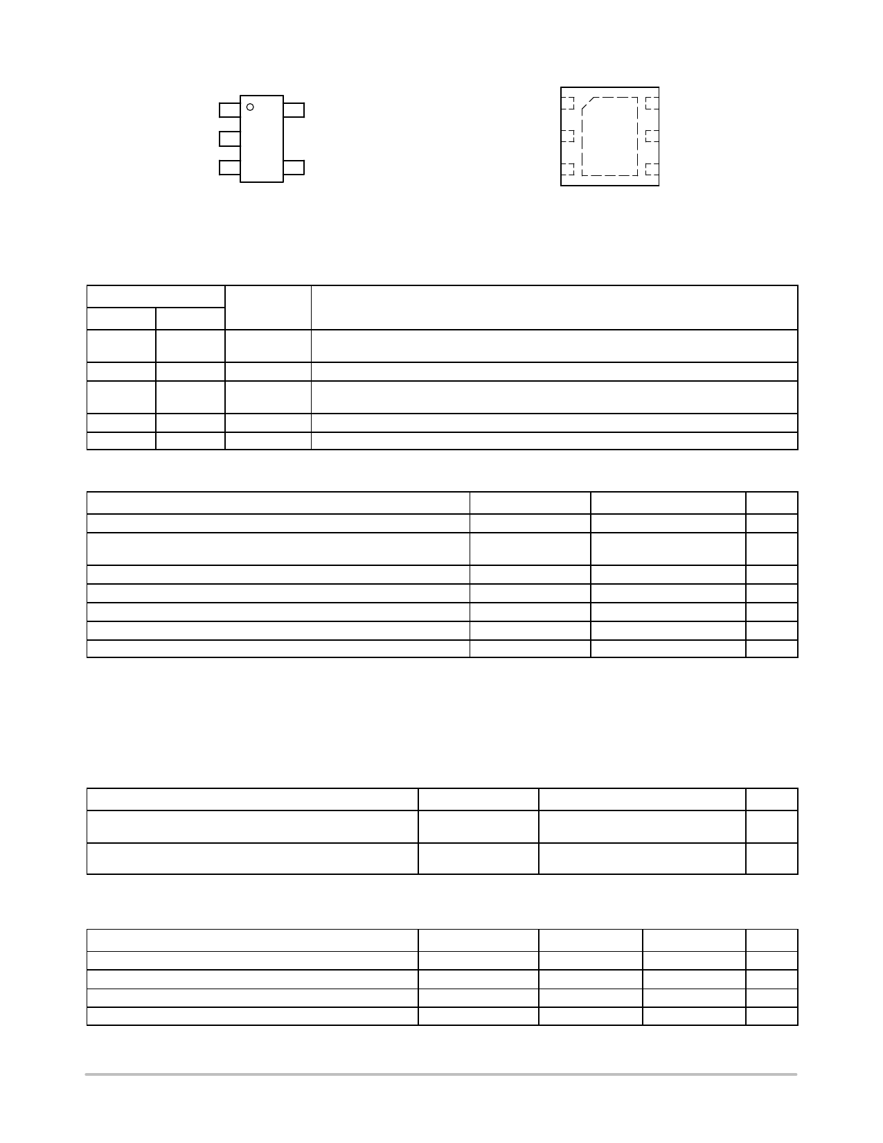
Vin 1
GND 2
5 Vout
PIN CONNECTIONS
Vout 1
GND 2
GND
6 Vin
5 GND
ENABLE 3
4 ADJ/NC*
(Top View)
* ADJ − Adjustable Version
* NC − Fixed Voltage Version
Figure 2. Pin Connections − TSOP5
NC 3
4 ENABLE
(Top View)
Figure 3. Pin Connections − DFN6
PIN FUNCTION DESCRIPTION
Pin No.
ÁÁÁÁ DFN6
TSOP−5 Pin Name
Description
ÁÁÁÁ 3
4
ADJ/NC Output Voltage Adjust Input (Adjustable Version), No Connection (Fixed Voltage Versions)
ÁÁÁÁ (Note 1)
2, 5, EPAD
2
GND
Power Supply Ground; Device Substrate
ÁÁÁÁ 4
3
ENABLE The Enable Input places the device into low−power standby when pulled to logic low
ÁÁÁÁ (< 0.4 V). Connect to Vin if the function is not used.
ÁÁÁÁ 6
1
Vin
Positive Power Supply Input
ÁÁÁÁ 1
5
Vout
Regulated Output Voltage
ÁÁÁÁ 1. True no connect. Printed circuit board traces are allowable.
ABSOLUTE MAXIMUM RATINGS
Rating
Symbol
Value
Unit
Input Voltage Range (Note 2)
Output, Enable, Adjustable Voltage Range
Vin
−0.3 to 6.5
V
Vout, ENABLE, ADJ −0.3 to 6.5 (or Vin + 0.3)
V
Whichever is Lower
Maximum Junction Temperature
Storage Temperature Range
ESD Capability, Human Body Model (Note 3)
ESD Capability, Machine Model (Note 3)
Moisture Sensitivity Level
TJ(max)
TSTG
ESDHBM
ESDMM
MSL
150
°C
−65 to 150
°C
3500
V
200
V
MSL1/260
−
Stresses exceeding Maximum Ratings may damage the device. Maximum Ratings are stress ratings only. Functional operation above the
Recommended Operating Conditions is not implied. Extended exposure to stresses above the Recommended Operating Conditions may affect
device reliability.
2. Refer to ELECTRICAL CHARACTERISTICS and APPLICATION INFORMATION for Safe Operating Area.
3. This device series incorporates ESD protection and is tested by the following methods:
ESD Human Body Model tested per AEC−Q100−002 (EIA/JESD22−A114)
ESD Machine Model tested per AEC−Q100−003 (EIA/JESD22−A115)
Latchup Current Maximum Rating: v150 mA per JEDEC standard: JESD78.
THERMAL CHARACTERISTICS
Rating
Thermal Characteristics, DFN6, 2x2.2 mm (Note 4)
Thermal Resistance, Junction−to−Air (Note 5)
Thermal Characteristics, TSOP−5 (Note 4)
Thermal Resistance, Junction−to−Air (Note 5)
Symbol
RqJA
RqJA
Value
122
215
Unit
°C/W
°C/W
4. Refer to ELECTRICAL CHARACTERISTICS and APPLICATION INFORMATION for Safe Operating Area.
5. Values based on copper area of 645 mm2, 1 oz copper thickness.
OPERATING RANGES (Note 6)
Rating
Symbol
Min
Max
Unit
Operating Input Voltage (Note 7)
Adjustable Output Voltage (Adjustable Version Only)
Output Current
Ambient Temperature
Vin
1.75 V
6
V
Vout
1.25
5.0
V
Iout
0
150
mA
TA
−40
125
°C
6. Refer to ELECTRICAL CHARACTERISTICS and APPLICATION INFORMATION for Safe Operating Area.
7. Minimum Vin = 1.75 V or (Vout + VDO), whichever is higher.
http://onsemi.com
2
Share Link: 