AD743JR-16-REEL7 데이터 시트보기 (PDF) - Analog Devices
부품명
상세내역
일치하는 목록
AD743JR-16-REEL7 Datasheet PDF : 12 Pages
| |||
AD743
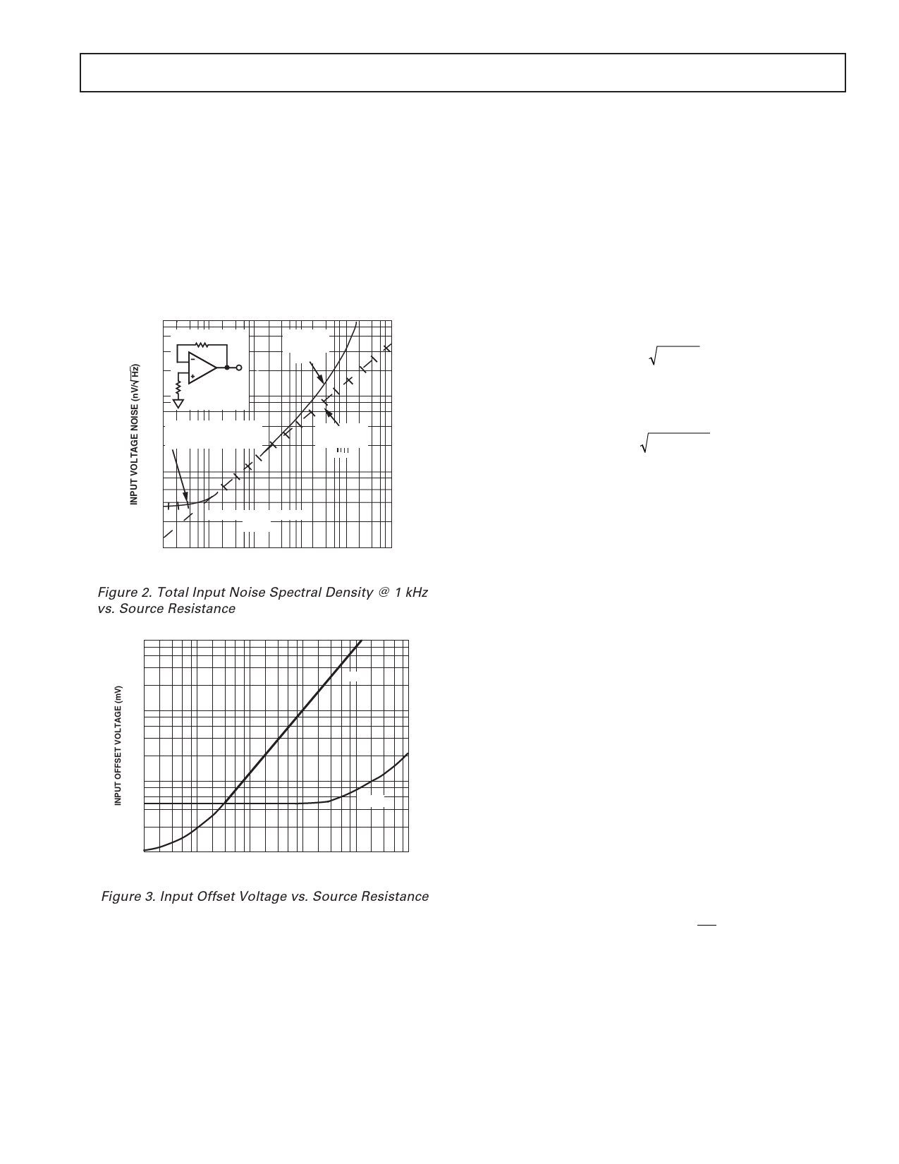
OP AMP PERFORMANCE: JFET VS. BIPOLAR
The AD743 is the first monolithic JFET op amp to offer the low
input voltage noise of an industry-standard bipolar op amp without
its inherent input current errors. This is demonstrated in Figure 2,
which compares input voltage noise versus input source resis-
tance of the OP27 and AD743 op amps. From this figure, it is
clear that at high source impedance the low current noise of the
AD743 also provides lower total noise. It is also important to
note that with the AD743 this noise reduction extends all the
way down to low source impedances. The lower dc current errors
of the AD743 also reduce errors due to offset and drift at high
source impedances (Figure 3).
1000
R SOURCE
EO
OP27 AND
RESISTOR
(—)
100
R SOURCE
AD743 AND RESISTOR
OR
OP27 AND RESISTOR
10
AD743 AND
RESISTOR
()
RESISTOR NOISE ONLY
(– – –)
1
100
1k
10k
100k
1M
10M
SOURCE RESISTANCE (⍀)
Figure 2. Total Input Noise Spectral Density @ 1 kHz
vs. Source Resistance
100
OP27
10
1
AD743
0.1
100
1k
10k
100k
1M
10M
SOURCE RESISTANCE (⍀)
Figure 3. Input Offset Voltage vs. Source Resistance
DESIGNING CIRCUITS FOR LOW NOISE
An op amp’s input voltage noise performance is typically divided
into two regions: flatband and low frequency noise. The AD743
offers excellent performance with respect to both. The figure of
2.9 nV/√Hz @ 10 kHz is excellent for a JFET input amplifier. The
0.1 Hz to 10 Hz noise is typically 0.38 µV p-p. The user should
pay careful attention to several design details in order to optimize
low frequency noise performance. Random air currents can gen-
erate varying thermocouple voltages that appear as low frequency
noise; therefore, sensitive circuitry should be well shielded from
air flow. Keeping absolute chip temperature low also reduces low
frequency noise in two ways. First, the low frequency noise is
strongly dependent on the ambient temperature and increases
above +25°C. Second, since the gradient of temperature from the
IC package to ambient is greater, the noise generated by random
air currents, as previously mentioned, will be larger in magnitude.
Chip temperature can be reduced both by operation at reduced
supply voltages and by the use of a suitable clip-on heat sink,
if possible.
Low frequency current noise can be computed from the magni-
tude of the dc bias current
˜In = 2qIB∆f
and increases below approximately 100 Hz with a 1/f power spectral
density. For the AD743, the typical value of current noise is
6.9 fA/√Hz at 1 kHz. Using the formula
I˜n = 4kT / R∆f
to compute the Johnson noise of a resistor, expressed as a current,
one can see that the current noise of the AD743 is equivalent to
that of a 3.45 ϫ 108 Ω source resistance.
At high frequencies, the current noise of a FET increases pro-
portionately to frequency. This noise is due to the “real” part of
the gate input impedance, which decreases with frequency. This
noise component usually is not important, since the voltage noise
of the amplifier impressed upon its input capacitance is an appar-
ent current noise of approximately the same magnitude.
In any FET input amplifier, the current noise of the internal
bias circuitry can be coupled externally via the gate-to-source
capacitances and appears as input current noise. This noise is
totally correlated at the inputs, so source impedance match-
ing will tend to cancel out its effect. Both input resistance and
input capacitance should be balanced whenever dealing with
source capacitances of less than 300 pF in value.
LOW NOISE CHARGE AMPLIFIERS
As stated, the AD743 provides both low voltage and low current
noise. This combination makes this device particularly suitable
in applications requiring very high charge sensitivity, such as
capacitive accelerometers and hydrophones. When dealing with
a high source capacitance, it is useful to consider the total input
charge uncertainty as a measure of system noise.
Charge (Q) is related to voltage and current by the simply stated
fundamental relationships
Q = CV and I = dQ
dt
As shown, voltage, current, and charge noise can all be directly
related. The change in open circuit voltage (∆V) on a capacitor
will equal the combination of the change in charge (∆Q/C) and
the change in capacitance with a built in charge (Q/∆C).
REV. E
–7–
Share Link: 