AD743JR-16-REEL7 데이터 시트보기 (PDF) - Analog Devices
부품명
상세내역
일치하는 목록
AD743JR-16-REEL7 Datasheet PDF : 12 Pages
| |||
R3
100⍀
CC
R4*
R2
1900⍀
C1*
B AND K TYPE 8100
HYDROPHONE
CT
R1
108⍀
AD743
OUTPUT
INPUT SENSITIVITY = –179 dB re. 1V/Pa**
*OPTIONAL, SEE TEXT
**1V PER MICROPASCAL
Figure 15b. AC-Coupled, Low Noise
Hydrophone Amplifier
R3
100⍀
R4*
108⍀
R2
1900⍀
C1*
AD743
OUTPUT
R7
16M⍀
B AND K
TYPE 8100
HYDROPHONE
CT
R1
108⍀
R6
1M⍀
R5
100k⍀
C2
0.27F
AD711K
16M⍀
DC OUTPUT Յ 1mV FOR IB (AD743) Յ 100nA
*OPTIONAL, SEE TEXT
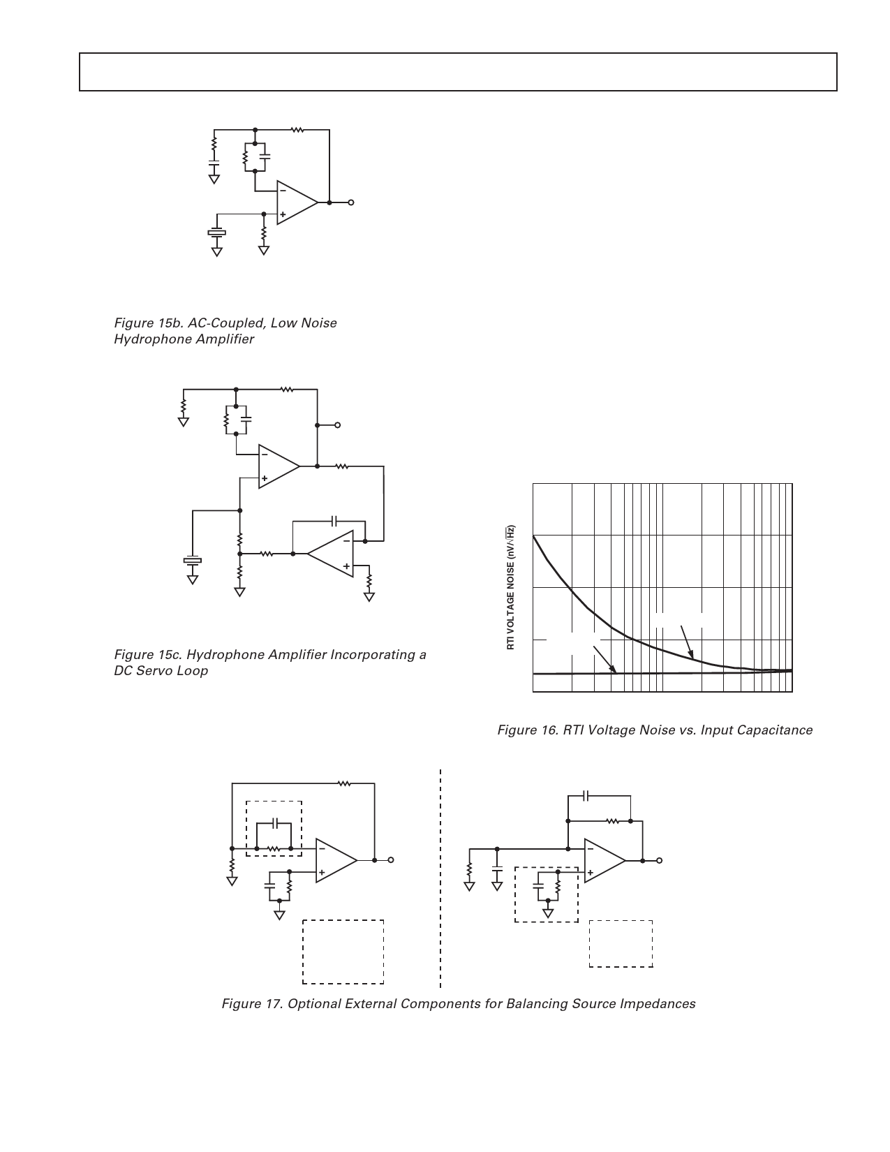
Figure 15c. Hydrophone Amplifier Incorporating a
DC Servo Loop
AD743
where the dc gain is 1 and the gain above the low frequency cutoff
(1/(2πCC(100 Ω))) is the same as the circuit of Figure 15a. The
circuit of Figure 15c uses a dc servo loop to keep the dc output
at 0 V and to maintain full dynamic range for IB up to 100 nA.
The time constant of R7 and C2 should be larger than that of
R1 and CT for a smooth low frequency response.
The transducer shown has a source capacitance of 7500 pF. For
smaller transducer capacitances (≤300 pF), the lowest noise can
be achieved by adding a parallel RC network (R4 = R1, C1 = CT)
in series with the inverting input of the AD743.
BALANCING SOURCE IMPEDANCES
As mentioned previously, it is good practice to balance the
source impedances (both resistive and reactive) as seen by the
inputs of the AD743. Balancing the resistive components will
optimize dc performance over temperature because balancing
will mitigate the effects of any bias current errors. Balancing
input capacitance will minimize ac response errors due to the
amplifier’s input capacitance and, as shown in Figure 16, noise
performance will be optimized. Figure 17 shows the required
external components for noninverting (A) and inverting (B)
configurations.
40
30
20
10 BALANCED
2.9nV/√Hz
UNBALANCED
10
100
1000
INPUT CAPACITORS (pF)
Figure 16. RTI Voltage Noise vs. Input Capacitance
R1
CF
CB
R1
RB
A
B
R2
OUTPUT
RS CS
CS
RS
NONINVERTING
CONNECTION
CB
RB
OUTPUT
INVERTING
CONNECTION
A
CB = CS
RB = RS
FOR
RS >> R1 OR R2
B
CB = CF ʈ CS
RB = R1 ʈ RS
Figure 17. Optional External Components for Balancing Source Impedances
REV. E
–11–
Share Link: 