FX805 데이터 시트보기 (PDF) - CML Microsystems Plc
부품명
상세내역
일치하는 목록
FX805 Datasheet PDF : 17 Pages
| |||
Application Information ......
External Components ......
Figure 3 shows an input component configuration for use
generally for CTCSS signal and NRZ data reception.
Input coupling capacitor C is required because the Rx
3
Sub-Audio Input is held at V during all powered conditions
BIAS
of the FX805. Diodes D and D can be any silicon small-
1
2
signal diode.
The output resistance (open loop) of the on-chip Rx Amp
is ≈ 6kΩ. In the configuration shown in Figure 3, the (Rx
Amp) RC time-constant is therefore 90ms. If this period is
too long for some systems, ie. those employing half-duplex,
short data bursts, an external amplifier should be considered
in place of the FX805 on-chip Rx Amp.
From
Rx Discriminator
FX805 Rx LPF
14
Rx AMP IN
13
FX805
Rx AMP
+
–
C9
R9
16
15
17 EXTERNAL
OP-AMP
+
–
R2
D2
D.C. RESTORATION
R5
C4
R10
R11
VDD
VSS
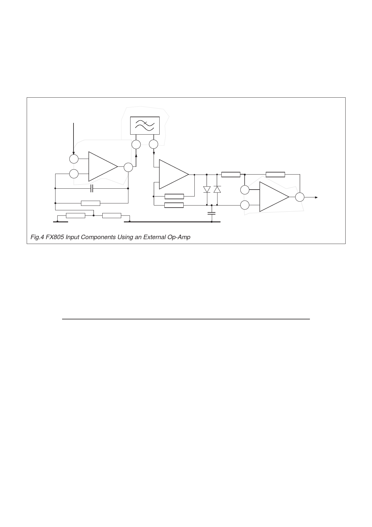
Fig.4 FX805 Input Components Using an External Op-Amp
FX805
COMPARATOR
R3
R4
D1
20
+
COMPARATOR IN
19
–
21
COMPARATOR OUT
HYSTERESIS
Using an External Op-Amp
For d.c. coupling the FX805 to the receiver’s discriminator
output when using NRZ communication, it is recommended
that an additional, external Op-Amp is employed as
configured in Figure 4. This configuration will allow long
sequences of logic “1s” or “0s” to be successfully decoded
(eg. LTR™ trunking systems).
Components R , R and R should be calculated to
9 10
11
provide an accurate potential of 2.5V d.c. (equal to V ) at
BIAS
pin-junction 15/16 when using a discriminator input. C is an
9
optional component which, if additional filtering is required,
should be calculated, with R9 to provide a lowpass cut-off
frequency (f ) of 500Hz.
CO
LTR™ is a registered trademark of E.F. Johnson Company
FX805 Operational Modes
NRZ Tx (Encoding)
The NRZ Encoder is formed by a shift register and the Tx
Sub-Audio Lowpass Filter. Data loaded from the Command
Data line is output one 8-bit byte at a time from the NRZ Tx
Data Register. The output data-signal level may be adjusted
and filtered. Data may be pre-emphasized via a “C-BUS”
command. The Tx baud rate is programmed as the NRZ Tx
Baud Rate (R ) (Table 5).
NRZ Tx
NRZ Rx (Decoding)
Input (NRZ type) sub-audio signals are filtered and the
data clock extracted. Decoded data is serially loaded into a
shift register buffer. This data is output one 8-bit byte at a
time as Reply Data from the NRZ Rx Data Register (Page
14) to the µController. The expected Rx baud rate is
programmed as the NRZ Rx Baud Rate (R ) (Table 5).
NRZ Rx
Any codeword recognition can be carried out by software.
CTCSS Tx (Encoding)
The CTCSS Tone Encoder comprises a clock-divider
programmed by an 11-bit binary number (Q) loaded to the
CTCSS Tx Frequency Register (Table 5) via the “C-BUS”
Command Data line.
The square-wave output of the encoder is fed through the
Tx Level Adjust variable gain block to the Tx Sub-Audio
Lowpass Filter, a variable bandwidth circuit controlled by
4-bits (P) of the CTCSS Tx Frequency Register. The Tx Sub-
Audio output is a sine-wave. Standard and non-standard
sub-audio tones are available, a ‘CDCS’ turn-off tone may be
generated.
CTCSS Rx ( Decoding)
Received CTCSS signals are filtered, coherence is
increased by the digital noise filter. The quality of the signal
is assessed by measurement of the cycle-to-cycle period
variance and, provided it is sufficiently good, the frequency is
measured over a period of 122.64 milliseconds.
If the average signal quality is consistently too low, NOTONE
is indicated, if not, the input frequency is precisely indicated
in the CTCSS Rx Frequency Register in a binary form as
shown in Figure 6.
As any single sub-audio tone within the specified range
may be selected, this would enable a ‘CDCS’ turn-off tone
(of 134Hz) to be decoded whilst operating in the NRZ Rx
mode.
5
Share Link: 