CDP1877 데이터 시트보기 (PDF) - Intersil
부품명
상세내역
일치하는 목록
CDP1877 Datasheet PDF : 10 Pages
| |||
CDP1877, CDP1877C
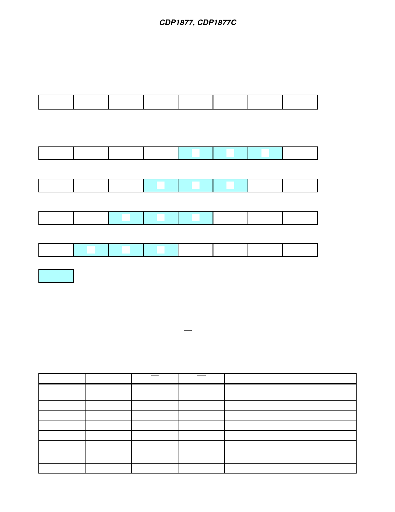
Second (High-Order Address) Byte
This byte is the High-Order vector Address that was written
into the PIC’s Page Register by the user. The PIC does not
alter this value in any way.
High-Order Vector Address
BUS 7
A15
A14
A13
A12
A11
A10
Third (Low-Order Address) Bytes
INTERVAL 2
BUS 7
A7
A6
A5
A4
I2
I1
INTERVAL 4
BUS 7
A7
A6
A5
I2
I1
I0
INTERVAL 8
BUS 7
A7
A6
I2
I1
I0
0
INTERVAL 16
BUS 7
A7
I2
I1
I0
0
0
BUS 0
A9
A8
BUS 0
I0
0
BUS 0
0
0
BUS 0
0
0
BUS 0
0
0
Indicates active interrupt input number (binary 0 to 7).
Bits indicated by AX (x = 4 to 7) are the same as pro-
grammed into the control register. All other bits are
generated by the PIC.
REGISTER ADDRESSES
In order to read/write or obtain an interrupt vector from any
PIC in the system, all chip selects (CS/AX, CS/AY, CS, CS)
must be valid during TPA.
CS/AX and CS/AY are multiplexed addresses; both must be
high during TPA, and set according to this table during TPB
to access the proper register.
CS/AX
CS/AY
RD
WR
1
0
0
1
1
0
1
0
0
1
1
0
0
0
0
1
0
0
1
0
0
1
0
1
1
1
X
X
ACTION TAKEN
READ Long Branch instruction and vector for highest
priority unmasked interrupt pending.
WRITE to Page Register
WRITE to Control Register
READ Status Register
WRITE to Mask Register
READ Polling Register (Used to identify INTERRUPT
source if Polling technique rather than INTERRUPT ser-
vice is used.)
Unused condition
4-87
Share Link: 