CDP1877 데이터 시트보기 (PDF) - Intersil
부품명
상세내역
일치하는 목록
CDP1877 Datasheet PDF : 10 Pages
| |||
CDP1877, CDP1877C
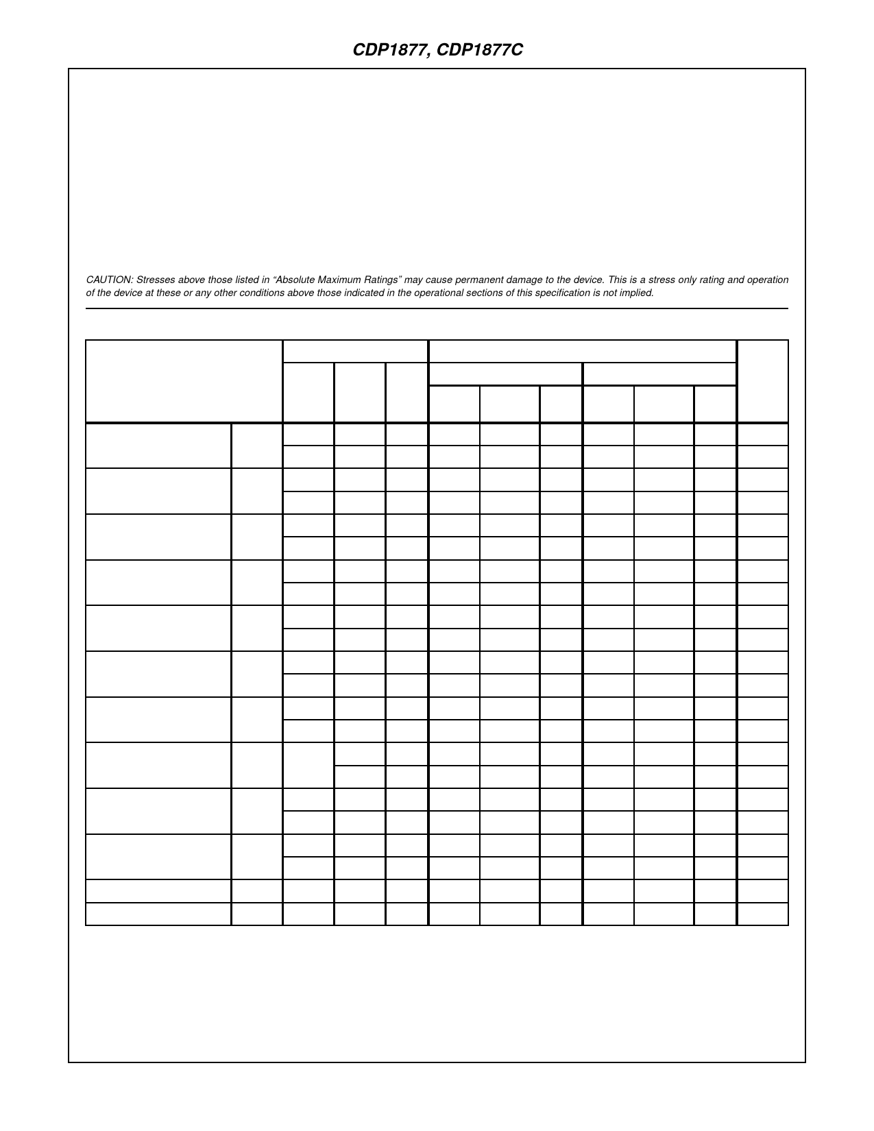
Absolute Maximum Ratings
Thermal Information
DC Supply-Voltage Range, (VDD)
(All Voltages Referenced to VSS Terminal)
CDP1877 . . . . . . . . . . . . . . . . . . . . . . . . . . . . . . . . . . -0.5V to +11V
CDP1877C . . . . . . . . . . . . . . . . . . . . . . . . . . . . . . . . . -0.5V to +7V
Input Voltage Range, All Inputs . . . . . . . . . . . . . -0.5V to VDD +0.5V
DC Input Current, Any One Input. . . . . . . . . . . . . . . . . . . . . . . . .±10mA
Thermal Resistance (Typical)
θJA (oC/W)
PDIP Package . . . . . . . . . . . . . . . . . . . . . . . . . . . . .
55
Device Dissipation Per Output Transistor
TA = Full Package Temperature Range
(All Package Types) . . . . . . . . . . . . . . . . . . . . . . . . . . . . . . 100mW
Operating Temperature Range (TA)
Package Type E . . . . . . . . . . . . . . . . . . . . . . . . . . . -40oC to +85oC
Storage Temperature Range (TSTG) . . . . . . . . . . . . -65oC to +150oC
Lead Temperature (During Soldering)
At distance 1/16 ± 1/32 In. (1.59 ± 0.79mm)
from case for 10s max . . . . . . . . . . . . . . . . . . . . . . . . . . . . +265oC
CAUTION: Stresses above those listed in “Absolute Maximum Ratings” may cause permanent damage to the device. This is a stress only rating and operation
of the device at these or any other conditions above those indicated in the operational sections of this specification is not implied.
Static Electrical Specifications At TA = -40 to +85oC, VDD ±5%, Unless Otherwise Specified
CONDITIONS
LIMITS
CDP1877
CDP1877C
PARAMETER
VO
VIN
VDD
(NOTE1)
(NOTE1)
(V)
(V)
(V) MIN
TYP MAX MIN
TYP MAX UNITS
Quiescent Device
Current
IDD
-
0, 5
5
-
0.01
50
-
0.02
200
µA
-
0, 10 10
-
1
200
-
-
-
µA
Output Low Drive (Sink)
IOL
0.4
0, 5
5
1.6
3.2
-
1.6
3.2
-
mA
Current
0.5
0, 10 10
2.6
5.2
-
-
-
-
mA
Output High Drive
(Source) Current
IOH
4.6
0, 5
5
-1.15
-2.3
9.5
0, 10 10
-2.6
-5.2
-
-1.15
-2.3
-
-
-
-
mA
-
mA
Output Voltage Low Level VOL
-
0, 5
5
-
(Note 2)
-
0, 10 10
-
0
0.1
-
0
0.1
-
0
0.1
V
-
-
V
Output Voltage High Level VOH
-
0, 5
5
4.9
5
-
4.9
5
-
V
(Note 2)
-
0, 10 10
9.9
10
-
-
-
-
V
Input Low Voltage
VIL 0.5, 4.5
-
5
-
0.5, 9.5
-
10
-
-
1.5
-
-
3
-
-
1.5
V
-
-
V
Input High Voltage
VIH 0.5, 4.5
-
5
3.5
-
-
3.5
-
-
V
0.5, 9.5
-
10
7
-
-
-
-
-
V
Input Leakage Current
IIN
Any
0, 5
5
-
Input
0, 10 10
-
-
±1
-
-
±2
-
-
±1
µA
-
-
µA
Three-State Output
Leakage Current
IOUT
0, 5
0, 5
5
-
±10-4
±1
-
±10-4
±1
µA
0, 10 0, 10 10
-
±10-4
±10
-
-
-
µA
Operating Device Current IOPER
-
(Note 3)
-
-
5
-
-
10
-
0.5
1.0
-
1.9
3.0
-
0.5
1.0
mA
-
-
mA
Input Capacitance
CIN
-
-
-
-
5
7.5
-
5
7.5
pF
Output Capacitance
COUT
-
-
-
-
10
15
-
10
15
pF
NOTES:
1. Typical values are for TA = +25oC and nominal VDD.
2. IOL = IOH = 1µA
3. Operating current is measured under worst-case conditions in a 3.2MHz CDP1802A system, one PIC access per instruction cycle.
4-83
Share Link: 