R6011KND3 데이터 시트보기 (PDF) - ROHM Semiconductor
부품명
상세내역
일치하는 목록
R6011KND3 Datasheet PDF : 16 Pages
| |||
R6011KND3
Datasheet
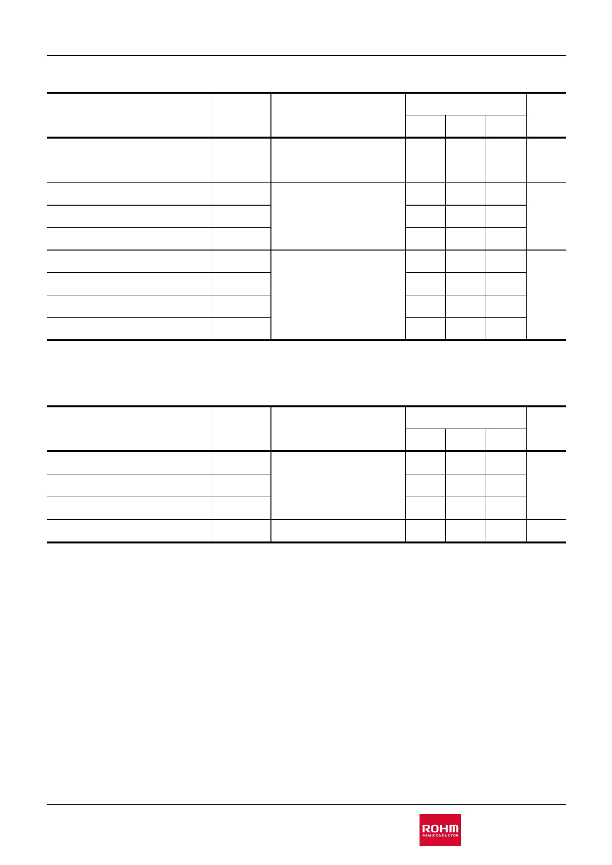
lElectrical characteristics (Ta = 25°C)
Parameter
Symbol
Conditions
Values
Unit
Min. Typ. Max.
Forward Transfer
Admittance
|Yfs|*6 VDS = 10V, ID = 5.5A
2.9 5.8 -
S
Input capacitance
Output capacitance
Reverse transfer capacitance
Turn - on delay time
Rise time
Turn - off delay time
Fall time
Ciss VGS = 0V
- 740 -
Coss VDS = 25V
- 630 - pF
Crss f = 1MHz
- 30 -
td(on)*6 VDD ⋍ 300V, VGS = 10V
-
20
-
tr*6
td(off)*6
ID = 5.5A
RL ⋍ 54.9Ω
- 25 -
ns
- 40 -
tf*6 RG = 10Ω
- 20 -
lGate charge characteristics (Ta = 25°C)
Parameter
Symbol
Conditions
Total gate charge
Gate - Source charge
Gate - Drain charge
Gate plateau voltage
Qg*6
Qgs*6
Qgd*6
V(plateau)
VDD ⋍ 300V
ID = 11A
VGS = 10V
VDD ⋍ 300V, ID = 11A
Values
Unit
Min. Typ. Max.
- 22 -
-
6
- nC
- 10 -
- 6.7 -
V
*1 Limited only by maximum channel temperature allowed.
*2 Pw ≤ 10μs, Duty cycle ≤ 1%
*3 L≒100mH, VDD=50V, RG=25Ω, STARTING Tj=25℃
*4 TC=25℃
*5 Mounted on a epoxy PCB FR4 (25mm x 27mm x 0.8mm)
*6 Pulsed
www.rohm.com
© 2018 ROHM Co., Ltd. All rights reserved.
3/12
20180612 - Rev.001
Share Link: 