BR24G64XXX-5 데이터 시트보기 (PDF) - ROHM Semiconductor
부품명
상세내역
일치하는 목록
BR24G64XXX-5 Datasheet PDF : 37 Pages
| |||
BR24G64xxx-5 Series
Pin Configuration
A0 1
A1 2
A2 3
GND 4
(TOP VIEW)
88 VCC
7 WP
6 SCL
5 SDA
Figure 3-(a). Pin Configuration
(SOP8, SOP-J8, TSSOP-B8, MSOP8)
A0 1
A1 2
A2 3
GND 4
(TOP VIEW)
EXP-PAD
8 VCC
7 WP
6 SCL
5 SDA
Figure 3-(b). Pin Configuration
(VSON008X2030)
Pin Description
Pin No.
Pin Name
Input / Output
Descriptions
1
A0
Input
Slave address setting(Note 1)
2
A1
Input
Slave address setting(Note 1)
3
A2
Input
Slave address setting(Note 1)
4
GND
-
Reference voltage of all input / output, 0V
5
SDA
Input / Output Serial data input / serial data output(Note 2)
6
SCL
Input
Serial clock input
7
WP
Input
Write protect pin(Note 3)
8
VCC
-
Connect the power source
-
EXP-PAD
-
Leave as OPEN or connect to GND
(Note 1) Connect to VCC or GND. There are pull-down elements inside the IC. If pins are open, they are the same as when they are connected to GND.
(Note 2) SDA is NMOS open drain, so it requires a pull-up resistor.
(Note 3) Connect to VCC or GND, or control to 'HIGH' level or 'LOW' level. There are pull-down elements inside the IC. If this pin is open, this input is recognized
as 'LOW'.
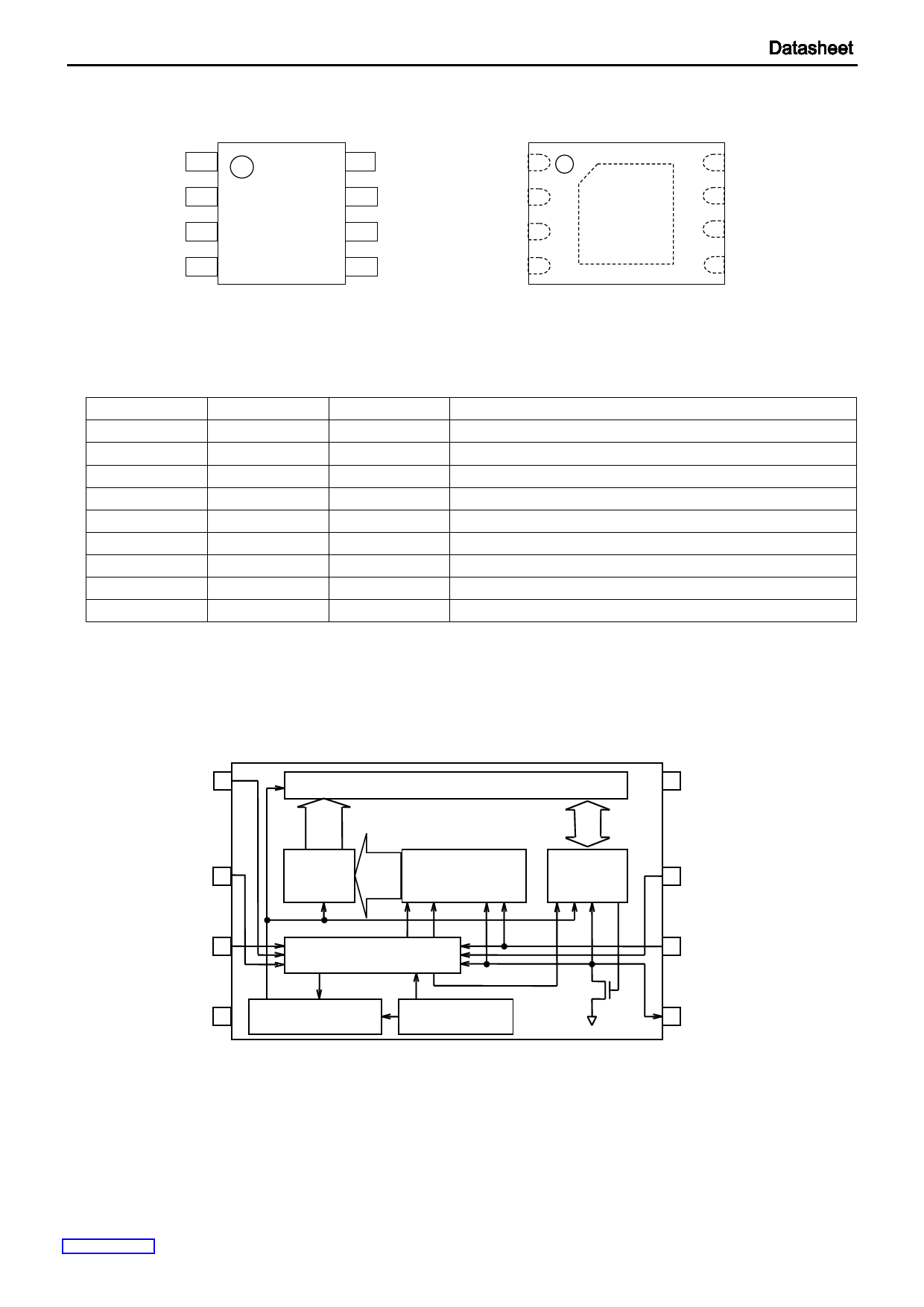
Block Diagram
A0 1
A1 2
64Kbit EEPROM Array
Address
Decoder 13bit
Word
Address Register
8bit
Data
Register
A2 3
GND 4
START
Control Circuit
STOP
ACK
High Voltage
Generating Circuit
Supply Voltage
Detection
Figure 4. Block Diagram
8 VCC
7 WP
6 SCL
5 SDA
www.rohm.com
© 2017 ROHM Co., Ltd. All rights reserved.
TSZ22111 • 15 • 001
3/34
TSZ02201-0GGG0G100910-1-2
05.Jun.2020 Rev.003
Share Link: 