BR24G64NUX-5(2017) 데이터 시트보기 (PDF) - ROHM Semiconductor
부품명
상세내역
일치하는 목록
BR24G64NUX-5
(Rev.:2017)
(Rev.:2017)
ROHM Semiconductor

BR24G64NUX-5 Datasheet PDF : 38 Pages
| |||
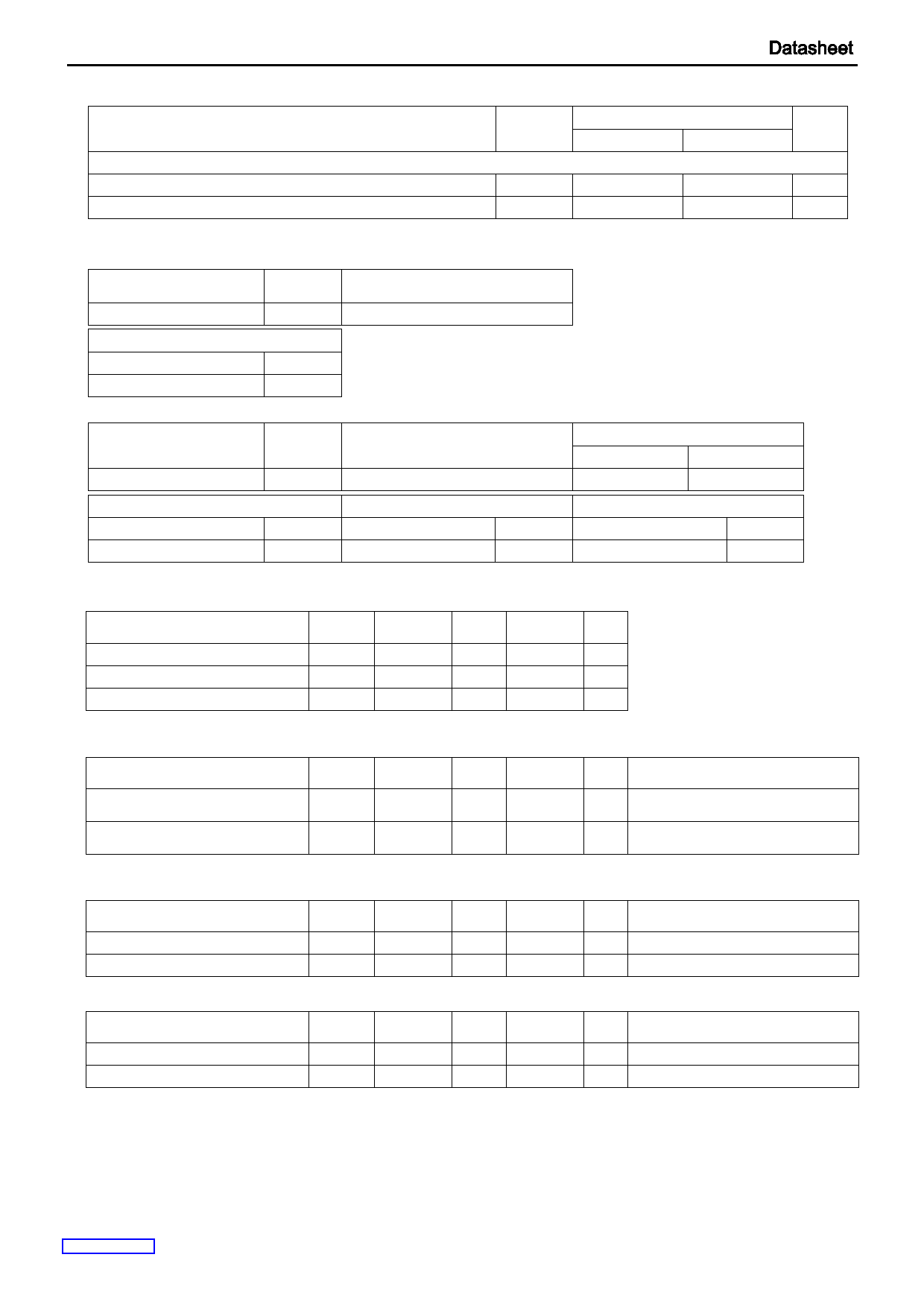
BR24G64xxx-5 Series
Thermal Resistance(Note 8) - continued
Parameter
Symbol
Thermal Resistance (Typ)
1s(Note 10)
2s2p(Note 11)
Unit
VSON008X2030
Junction to Ambient
θJA
308.3
69.6
°C/W
Junction to Top Characterization Parameter(Note 9)
ΨJT
43
10
°C/W
(Note 8) Based on JESD51-2A(Still-Air)
(Note 9) The thermal characterization parameter to report the difference between junction temperature and the temperature at the top center of the outside
surface of the component package.
(Note 10) Using a PCB board based on JESD51-3.
Layer Number of
Measurement Board
Material
Board Size
Single
FR-4
114.3mm x 76.2mm x 1.57mmt
Top
Copper Pattern
Footprints and Traces
Thickness
70μm
(Note 11) Using a PCB board based on JESD51-5, 7.
Layer Number of
Measurement Board
Material
Board Size
4 Layers
FR-4
114.3mm x 76.2mm x 1.6mmt
Top
2 Internal Layers
Copper Pattern
Thickness
Copper Pattern
Thickness
Footprints and Traces
70μm
74.2mm x 74.2mm
(Note 12) This thermal via connects with the copper pattern of all layers.
35μm
Thermal Via(Note 12)
Pitch
Diameter
1.20mm
Φ0.30mm
Bottom
Copper Pattern
74.2mm x 74.2mm
Thickness
70μm
Operating Conditions
Parameter
Symbol
Min
Typ
Supply Voltage
VCC
1.6
-
Ambient Operating Temperature
Ta
-40
-
Bypass capacitor(Note 13)
C
0.1
-
(Note 13) Connect a bypass capacitor between the IC’s VCC and GND pin.
Max Unit
5.5
V
+85
°C
-
µF
Input / Output Capacitance (Ta=25°C, f=1MHz)
Parameter
Symbol
Min
Typ
Max Unit
Conditions
Input / Output Capacitance
(SDA)(Note 14)
CI/O
-
-
8
pF VI/O=GND
Input Capacitance
(SCL, A0, A1, A2, WP)(Note 14)
CIN
-
-
8
pF VIN=GND
(Note 14) Not 100% TESTED.
Input Impedance (Unless otherwise specified, Ta=-40°C to +85°C, VCC=1.6V to 5.5V)
Parameter
Symbol
Min
Typ
Max Unit
Conditions
Input Impedance 1
Input Impedance 2
ZIH
500
-
ZIL
30
-
0.7VCC≤VIN (A0, A1, A2, WP)
-
kΩ Period from Start Condition to
Stop Condition
VIN≤0.3VCC (A0, A1, A2, WP)
-
kΩ Period from Start Condition to
Stop Condition
Memory Cell Characteristics (VCC=1.6V to 5.5V)
Parameter
Symbol
Min
Typ
Max Unit
Write Cycles(Note 15,16)
-
4,000,000 -
-
Times Ta=25°C
Data Retention(Note 15)
-
200
-
-
Years Ta=55°C
(Note 15) Not 100% TESTED.
(Note 16) The Write Cycles is defined for unit of 4 data bytes with the same address bits of WA12 to WA2.
Conditions
www.rohm.com
© 2017 ROHM Co., Ltd. All rights reserved.
TSZ22111 • 15 • 001
5/34
TSZ02201-0GGG0G100910-1-2
30.Nov.2017 Rev.001
Share Link: