ST6210LB1/OTP 데이터 시트보기 (PDF) - STMicroelectronics
부품명
상세내역
일치하는 목록
ST6210LB1/OTP
STMicroelectronics

ST6210LB1/OTP Datasheet PDF : 104 Pages
| |||
ST6208C/ST6209C/ST6210C/ST6220C
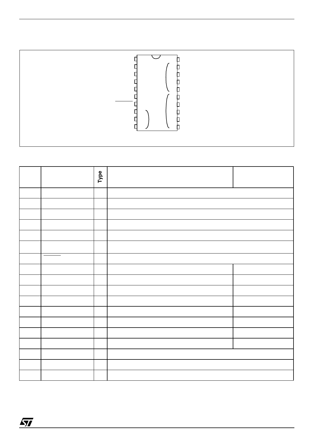
2 PIN DESCRIPTION
Figure 2. 20-Pin Package Pinout
VDD
TIMER
OSCin
OSCout
NMI
VPP
RESET
Ain*/PB7
Ain*/PB6
Ain*/PB5
1
20
2
19
3
it1 18
4
17
5
16
6
15
7
14
8
it2 13
9 it2
12
10
11
VSS
PA0/20mA Sink
PA1/20mA Sink
PA2/20mA Sink
PA3/20mA Sink
PB0/Ain*
PB1/Ain*
PB2/Ain*
PB3/Ain*
PB4/Ain*
itX associated interrupt vector
* Depending on device. Please refer to I/O Port section.
Table 1. Device Pin Description
Pin n°
Pin Name
1 VDD
2 TIMER
3 OSCin
4 OSCout
5 NMI
6 VPP
7 RESET
8 PB7/Ain*
9 PB6/Ain*
10 PB5/Ain*
11 PB4/Ain*
12 PB3/Ain*
13 PB2/Ain*
14 PB1/Ain*
15 PB0/Ain*
16 PA3/ 20mA Sink
17 PA2/ 20mA Sink
18 PA1/ 20mA Sink
Main Function
(after Reset)
Alternate Function
S Main power supply
I/O Timer input or output
I External clock input or resonator oscillator inverter input
O Resonator oscillator inverter output or resistor input for RC oscillator
I Non maskable interrupt (falling edge sensitive)
Must be held at Vss for normal operation, if a 12.5V level is applied to the pin
during the reset phase, the device enters EPROM programming mode.
I/O Top priority non maskable interrupt (active low)
I/O Pin B7 (IPU)
Analog input
I/O Pin B6 (IPU)
Analog input
I/O Pin B5 (IPU)
Analog input
I/O Pin B4 (IPU)
Analog input
I/O Pin B3 (IPU)
Analog input
I/O Pin B2 (IPU)
Analog input
I/O Pin B1 (IPU)
Analog input
I/O Pin B0 (IPU)
Analog input
I/O Pin A3 (IPU)
I/O Pin A2 (IPU)
I/O Pin A1 (IPU)
7/104
5
Share Link: