AD7298-1BCPZ-RL 데이터 시트보기 (PDF) - Analog Devices
부품명
상세내역
일치하는 목록
AD7298-1BCPZ-RL Datasheet PDF : 24 Pages
| |||
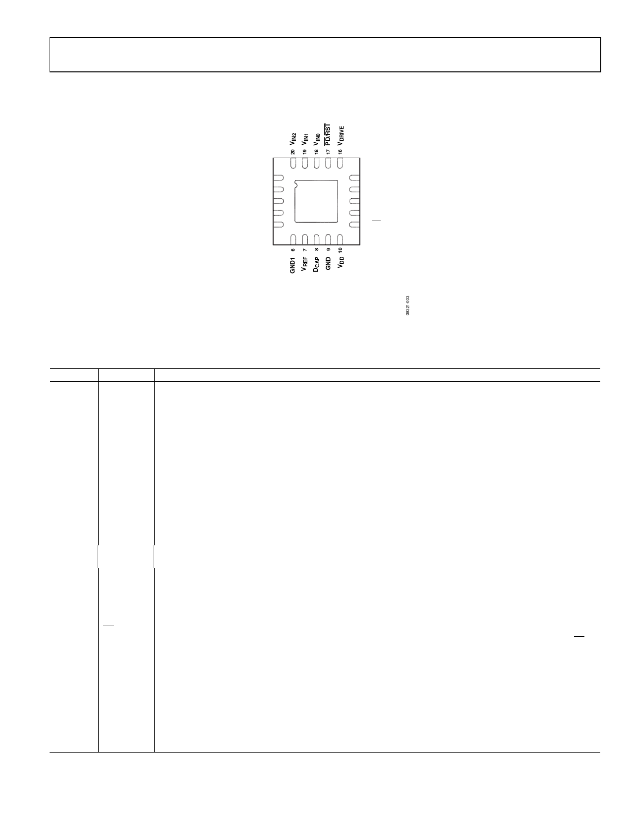
PIN CONFIGURATION AND FUNCTION DESCRIPTION
AD7298-1
VIN3 1
VIN4 2
VIN5 3
VIN6 4
VIN7 5
AD7298-1
TOP VIEW
(Not to Scale)
15 SCLK
14 DOUT
13 DIN
12 NC
11 CS
NOTES
1. NC = NO CONNECT.
2. THE EXPOSED METAL PADDLE ON THE BOTTOM
OF THE LFCSP PACKAGE SHOULD BE SOLDERED
TO PCB GROUND FOR PROPER FUNCTIONALITY
AND HEAT DISSIPATION.
Figure 2. Pin Configuration
Table 5. Pin Function Descriptions
Pin No. Mnemonic Description
1 to 5,
18 to 20
6
VIN3, VIN4
VIN5, VIN6,
VIN7, VIN0,
VIN1, VIN2
GND1
Analog Inputs. The AD7298-1 has eight single-ended analog inputs that are multiplexed into the on-chip track-
and-hold. Each input channel can accept analog inputs from 0 V to 2.5 V. Any unused input channels should be
connected to GND1 to avoid noise pickup.
Ground. Ground reference point for the internal reference circuitry on the AD7298-1. The external reference
signals and all analog input signals should be referred to the GND1 voltage. The GND1 pin should be connected
to the ground plane of a system. All ground pins should ideally be at the same potential and must not be more
than 0.3 V apart, even on a transient basis. The VREF pin should be decoupled to this ground pin via a 10 µF
decoupling capacitor.
7
VREF
Internal Reference/External Reference Supply. The nominal internal reference voltage of 2.5 V appears at this pin.
Provided the output is buffered, the on-chip reference can be taken from this pin and applied externally to the
rest of a system. Decoupling capacitors should be connected to this pin to decouple the reference buffer. For
best performance, it is recommended to use a 10 µF decoupling capacitor on this pin to GND1. The internal
reference can be disabled and an external reference supplied to this pin, if required. The input voltage range for
the external reference is 2.0 V to 2.5 V.
8
DCAP
Decoupling Capacitor Pins. Decoupling capacitors (1 µF recommended) are connected to this pin to decouple
the internal LDO.
9
GND
Ground. Ground reference point for all analog and digital circuitry on the AD7298-1. The GND pin should be
connected to the ground plane of the system. All ground pins should ideally be at the same potential and must
not be more than 0.3 V apart, even on a transient basis. Both the DCAP and VDD pins should be decoupled to this
GND pin.
10
VDD
11
CS
Supply Voltage, 2.8 V to 3.6 V. This supply should be decoupled to GND with 10 µF and 100 nF decoupling capacitors.
Chip Select, Active Low Logic Input. This pin is edge triggered on the falling edge of this input, the track-and-
hold goes into hold mode, and a conversion is initiated. This input also frames the serial data transfer. When CS is
low, the output bus is enabled and the conversion result becomes available on the DOUT output.
12
NC
No Connect.
13
DIN
Data In, Logic Input. Data to be written to the AD7298-1 control register is provided on this input and is clocked
into the register on the falling edge of SCLK.
14
DOUT
Serial Data Output. The conversion result from the AD7298-1 is provided on this output as a serial data stream.
The bits are clocked out on the falling edge of the SCLK input. The data stream from the AD7298-1 consists of
four address bits indicating which channel the conversion result corresponds to, followed by the 10 bits of
conversion data (MSB first).
15
SCLK
Serial Clock, Logic Input. A serial clock input provides the SCLK for accessing the data from the AD7298-1.
Rev. A | Page 7 of 24
Share Link: 