AD7298-1BCPZ-RL 데이터 시트보기 (PDF) - Analog Devices
부품명
상세내역
일치하는 목록
AD7298-1BCPZ-RL Datasheet PDF : 24 Pages
| |||
AD7298-1
TIMING SPECIFICATIONS
VDD = 2.8 V to 3.6 V, VDRIVE = 1.65 V to 3.6 V, VREF = 2.5 V internal, TA = −40°C to +125°C, unless otherwise noted. Sample tested during
initial release to ensure compliance. All input signals are specified with tr = tf = 5 ns (10% to 90% of VDRIVE) and timed from a voltage level
of 1.6 V.
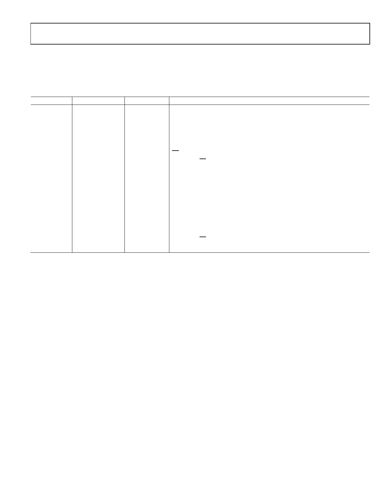
Table 2.
Parameter
tCONVERT
fSCLK1
tQUIET
Limit at TMIN, TMAX
t2 + (16 × tSCLK)
820
50
20
6
Unit
µs max
ns typ
kHz min
MHz max
ns min
t2
t31
t41
t5
t6
t71
t81
t9
t10
t111
tPOWER-UP
10
15
35
28
0.4 × tSCLK
0.4 × tSCLK
14
16/34
5
4
30
6
ns min
ns max
ns max
ns max
ns min
ns min
ns min
ns min/ns max
ns min
ns min
ns max
ms max
1 Measured with a load capacitance on DOUT of 15 pF.
Test Conditions/Comments
Conversion time
Each ADC channel VIN0 to VIN7, fSCLK = 20 MHz
Frequency of external serial clock
Frequency of external serial clock
Minimum quiet time required between the end of the serial read and the start of
the next voltage conversion in repeat and nonrepeat mode.
CS to SCLK setup time
Delay from CS (falling edge) until DOUT three-state disabled
Data access time after SCLK falling edge
VDRIVE = 1.65 V to 3 V
VDRIVE = 3 V to 3.6 V
SCLK low pulse width
SCLK high pulse width
SCLK to DOUT valid hold time
SCLK falling edge to DOUT high impedance
DIN setup time prior to SCLK falling edge
DIN hold time after SCLK falling edge
Delay from CS rising edge to DOUT high impedance
Internal reference power-up time from full power-down
Rev. A | Page 5 of 24
Share Link: 