MB88152A 데이터 시트보기 (PDF) - Cypress Semiconductor
부품명
상세내역
일치하는 목록
MB88152A Datasheet PDF : 25 Pages
| |||
MB88152A
9. Recommended Operating Conditions
Parameter
Symbol
Pin
Conditions
Power supply voltage VDD
“H” level input voltage VIH
“L” level input voltage VIL
Input clock
duty cycle
Input clock
slew rate
Operating
temperature
tDCI
SRIN
Ta
VDD
SEL,
FREQ/FREQ0,
XENS/FREQ1
XIN
SEL,
FREQ/FREQ0,
XENS/FREQ1
XIN
XIN
XIN
−
−
−
16.6 MHz to 100 MHz
100 MHz to 134 MHz
−
16.6 MHz to 100 MHz
100 MHz to 134 MHz
16.6 MHz to 100 MHz
100 MHz to 134 MHz
Input frequency
40 MHz to 100 MHz
Input frequency
100 MHz to 134 MHz
−
Min
3.0
VDD x 0.8
Value
Typ
3.3
−
(VSS = 0.0 V)
Max
3.6
VDD + 0.3
Unit
V
V
VDD x 0.8 −
VDD x 0.9 −
VSS
−
VDD + 0.3 V
VDD + 0.3 V
VDD x 0.2 V
VSS
−
VSS
−
40
50
45
50
0.0475 x fin −
− 1.75
3
−
−40
−
VDD x 0.2
VDD x 0.1
60
55
−
−
+ 85
V
V
%
V/ns
⋅C
WARNING:
The recommended operating conditions are required in order to ensure the normal operation of the semiconductor
device. All of the device's electrical characteristics are warranted when the device is operated within these ranges.
Always use semiconductor devices within their recommended operating condition ranges. Operation outside these
ranges may adversely affect reliability and could result in device failure.
No warranty is made with respect to uses, operating conditions, or combinations not represented on the data sheet.
Users considering application outside the listed conditions are advised to contact their representatives beforehand.
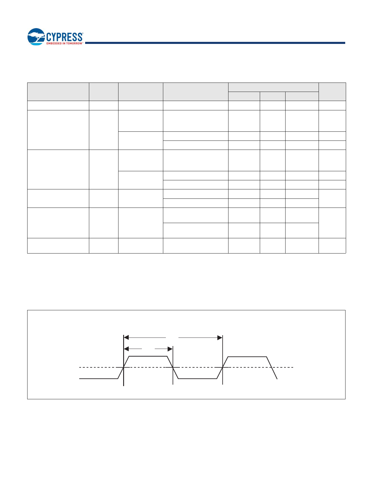
Input clock duty cycle (tDCI = tb/ta)
XIN
ta
tb
1.5 V
Document Number: 002-08308 Rev. *B
Page 10 of 24
Share Link: 