MAX186ACAP(2012) 데이터 시트보기 (PDF) - Maxim Integrated
부품명
상세내역
일치하는 목록
MAX186ACAP Datasheet PDF : 25 Pages
| |||
MAX186/MAX188
Low-Power, 8-Channel,
Serial 12-Bit ADCs
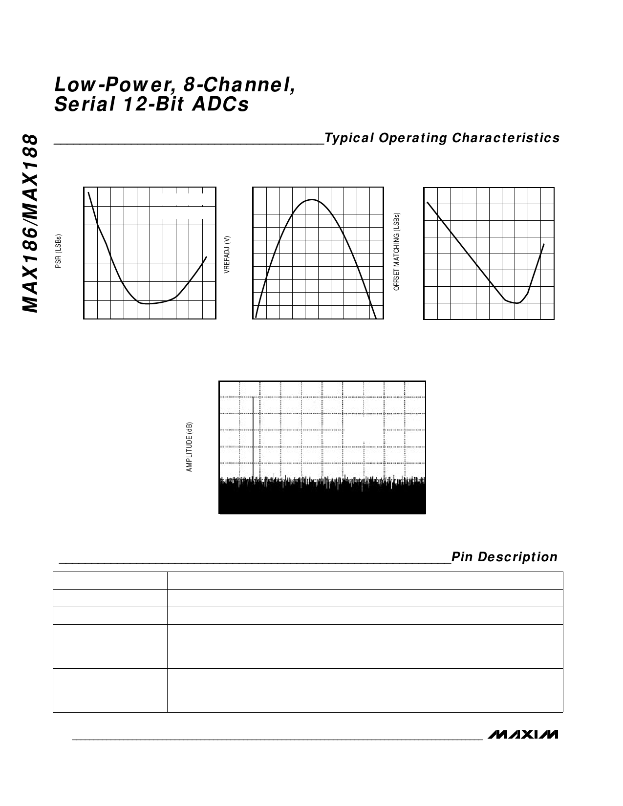
__________________________________________Typical Operating Characteristics
POWER-SUPPLY REJECTION
vs. TEMPERATURE
0.30
VDD = +5V ±5%
0.25
VSS = 0V or -5V
0.20
0.15
0.10
0.05
0.00
-0.05
-60 -40 -20 0 20 40 60 80 100 120 140
TEMPERATURE (°C)
INTERNAL REFERENCE VOLTAGE
vs. TEMPERATURE
2.456
2.455
2.454
2.453
2.452
-40 -20 0 20 40 60 80 100 120
TEMPERATURE (°C)
CHANNEL-TO-CHANNEL OFFSET MATCHING
vs. TEMPERATURE
0.16
0.14
0.12
0.10
0.08
0.06
0.04
0.02
0
-60 -40 -20 0 20 40 60 80 100 120 140
TEMPERATURE (°C)
MAX186/MAX188 FFT PLOT – 133kHz
20
0
-20
-40
-60
-80
-100
-120
-140
0
ft = 10kHz
ft =fs10=k1H3z3kHz
fs = 133kHz
TA = +25°C
33.25kHz
FREQUENCY
66.5kHz
_____________________________________________________________Pin Description
PIN
NAME
FUNCTION
1–8
CH0–CH7 Sampling Analog Inputs
9
VSS
Negative Supply Voltage. Connect to -5V ±5% or AGND
Three-Level Shutdown Input. Pulling SHDN low shuts the MAX186/MAX188 down to 10μA (max)
10
SHDN
supply current, otherwise the MAX186/MAX188 are fully operational. Pulling SHDN high puts the
reference-buffer amplifier in internal compensation mode. Leaving SHDN unconnected puts the
reference-buffer amplifier in external compensation mode.
Reference Voltage for analog-to-digital conversion. Also, output of the reference buffer amplifier
11
VREF (4.096V in the MAX186, 1.638 x REFADJ in the MAX188). Add a 4.7μF capacitor to ground when
using external compensation mode. Also functions as an input when used with a precision external
6
Maxim Integrated
Share Link: 