AV9248-127 데이터 시트보기 (PDF) - Integrated Circuit Systems
부품명
상세내역
일치하는 목록
AV9248-127 Datasheet PDF : 14 Pages
| |||
ICS9248 - 127
Absolute Maximum Ratings
Supply Voltage . . . . . . . . . . . . . . . . . . . . . . . . . . 5.5 V
Logic Inputs . . . . . . . . . . . . . . . . . . . . . . . . . . . . GND –0.5 V to VDD +0.5 V
Ambient Operating Temperature . . . . . . . . . . . . 0°C to +70°C
Case Temperature . . . . . . . . . . . . . . . . . . . . . . . . 115°C
Storage Temperature . . . . . . . . . . . . . . . . . . . . . . –65°C to +150°C
Stresses above those listed under Absolute Maximum Ratings may cause permanent damage to the device. These ratings are
stress specifications only and functional operation of the device at these or any other conditions above those listed in the
operational sections of the specifications is not implied. Exposure to absolute maximum rating conditions for extended
periods may affect product reliability.
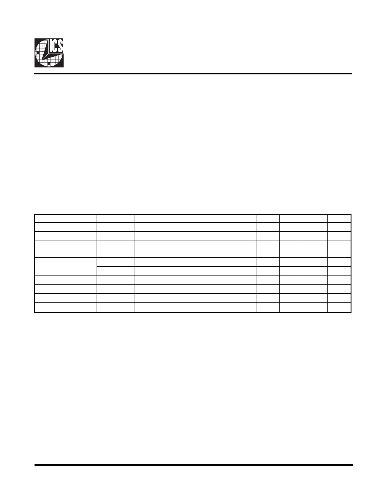
Electrical Characteristics - Input/Supply/Common Output Parameters
TA = 0 - 70C; Supply Voltage VDD = 3.3 V +/-5% (unless otherwise stated)
PAR AM ETER
SYM B OL
C ONDIT IONS
M IN TYP MAX UNITS
Input High Voltage
VIH
Input Low Voltage
VIL
Supply Current
IDD3.3 CL = 0 pF; Select @ 66M
Input frequency
Fi
VDD = 3.3 V;
Input Capacitance1
Transition Time1
Settling Time1
Clk Stabilization1
Skew1
C IN
C INX
Ttrans
Ts
TSTAB
T C PU-B US
Logic Inputs
X1 & X2 pins
To 1st crossing of target Freq.
From 1st crossing to 1% target Freq.
From VDD = 3.3 V to 1% target Freq.
VT = 1.5 V;
1Guarenteed by design, not 100% tested in production.
2
VDD+0 .3
VSS-0 .3
0 .8
77
180
1 4 .3 1 8
5
27
36
45
1 .5
3
3
1 .0
2 .2
4 .0
V
V
mA
M Hz
pF
pF
ms
ms
ms
ns
7
Share Link: 