SL74HC161 데이터 시트보기 (PDF) - System Logic Semiconductor
부품명
상세내역
일치하는 목록
SL74HC161 Datasheet PDF : 9 Pages
| |||
SL74HC161
VCC=Pin 16
GND=Pin 8
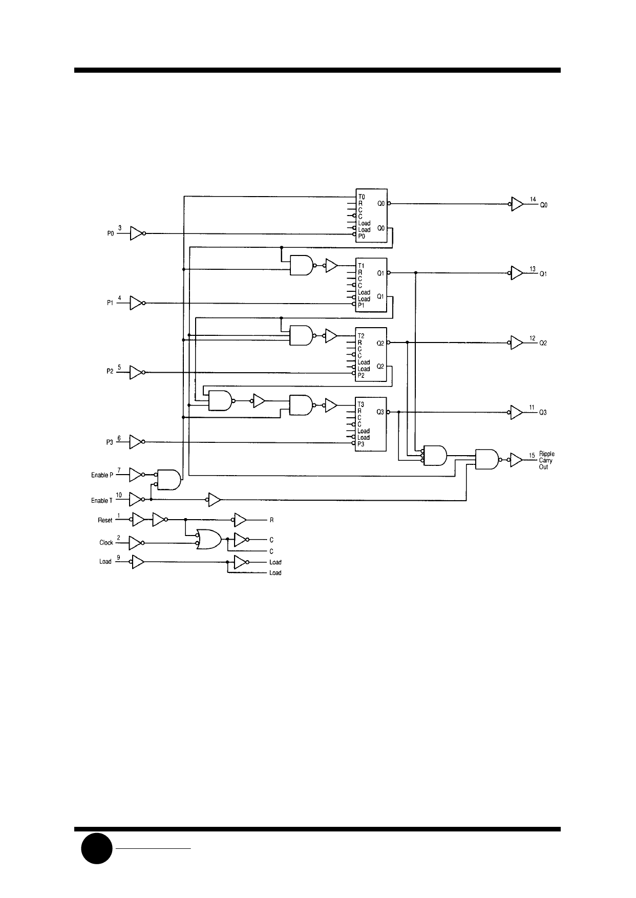
The flip-flops shown in the circuit diagrams are Toggle-Enable flip-flops. A Toggle-Enable flip-flop is a
combination of a D flip-flop and a T flip-flop. When loading data from Preset inputs P0, P1, P2, and P3, the Load
signal is used to disable the Toggle input (Tn) of the flip-flop. The logic level at the Pn input is then clocked to
the Q output of the flip-flop on the next rising edge of the clock.
A logic zero on the Reset device input forces the internal clock (C) high and resets the Q output of the flip-
flop low.
Figure 7.Expanded logic diagram
SLS
System Logic
Semiconductor
Share Link: 