MT9125AE 데이터 시트보기 (PDF) - Zarlink Semiconductor Inc
부품명
상세내역
일치하는 목록
MT9125AE Datasheet PDF : 18 Pages
| |||
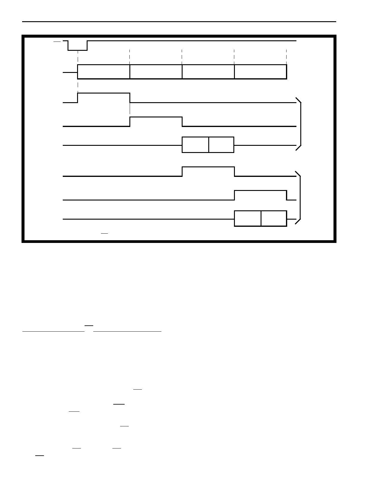
MT9125
F0i
DSTi/o
Channel 0
B1
Channel 1
B2
Preliminary Information
Channel 2
B1
Channel 3
B2
EN1
EN2
ADPCMi/o
B1
B2
ENS=0
EN1
EN2
ENS=1
ADPCMi/o
B1
B2
In ST-BUS mode the ENA, ENB1 and ENB2 input strobes are ignored. All timing is
dervied internally from the F0i, MCLK and ENS inputs.
Figure 4 - ST-BUS Mode Relative Timing
the device and must, therefore, be present whenever
a transcoding operation is required. These inputs
may be tied together and connected to the same
strobe for single channel operation. Only the B1
nibble is valid in this mode. Data is latched into the
DSTi pin with the falling edge of the bit clock while
output data is made available at DSTo on the rising
edge of the bit clock.
ST-BUS Conversion (F0i, C2o, EN1, EN2, ENS)
A simple converter circuit is incorporated which
allows ST-BUS signals to be converted to SSI
signals. In this manner it is very simple for an ST-
BUS application to be mixed with CODECs utilizing a
strobed data I/O.
This converter circuit consists of the F0i input and
C2o, EN1 and EN2 output pins (as well as the MCLK
input master clock). The output C4b clock and frame
pulse strobe (F0b), from the ST-BUS layer 1
transceiver, are connected directly to the master
clock (MCLK) and frame pulse (F0i) inputs of the
transcoder. A 2.048 MHz (C2o) bit clock output is
made available when a valid Frame Pulse is
connected to the F0i pin or the F0i pin is tied high. If
the F0i pin is tied low the C2o output is forced
continuously to a logic low level (not tri-stated).
Forcing the C2o output to logic low enhances power
conservation as well as removing a non-required
clock signal from the circuit. This 2.048 MHz bit clock
may be used to control external CODEC functions.
The 4.096 MHz and frame pulse signals are also
decoded into two output strobes corresponding to
the B1 and B2 channel timeslots of the ST-BUS.
These strobes (EN1 and EN2) are then used to
control the timing inputs of an external CODEC. A
typical example of this connection scheme is shown
in the application diagram of Figure 7.
The Enable Strobe pin (ENS) is used to position the
output strobes EN1 and EN2 within the ST-BUS
frame. Referring to Figure 4, when ENS=0 the output
strobes are positioned in channels 0 and 1 of the ST-
BUS frame. When ENS=1 the output strobes are
positioned in channels 2 and 3 of the ST-BUS frame.
This flexibility allows the transcoder to be used in ST-
BUS basic rate applications where channels 0 and 1
are defined as the D and C channels, respectively,
and also in line-card applications where the full
2.048 MHz bandwidth is used for conveying data
and/or digitally encoded voice information.
8-78
Share Link: 