MT9125AE 데이터 시트보기 (PDF) - Zarlink Semiconductor Inc
부품명
상세내역
일치하는 목록
MT9125AE Datasheet PDF : 18 Pages
| |||
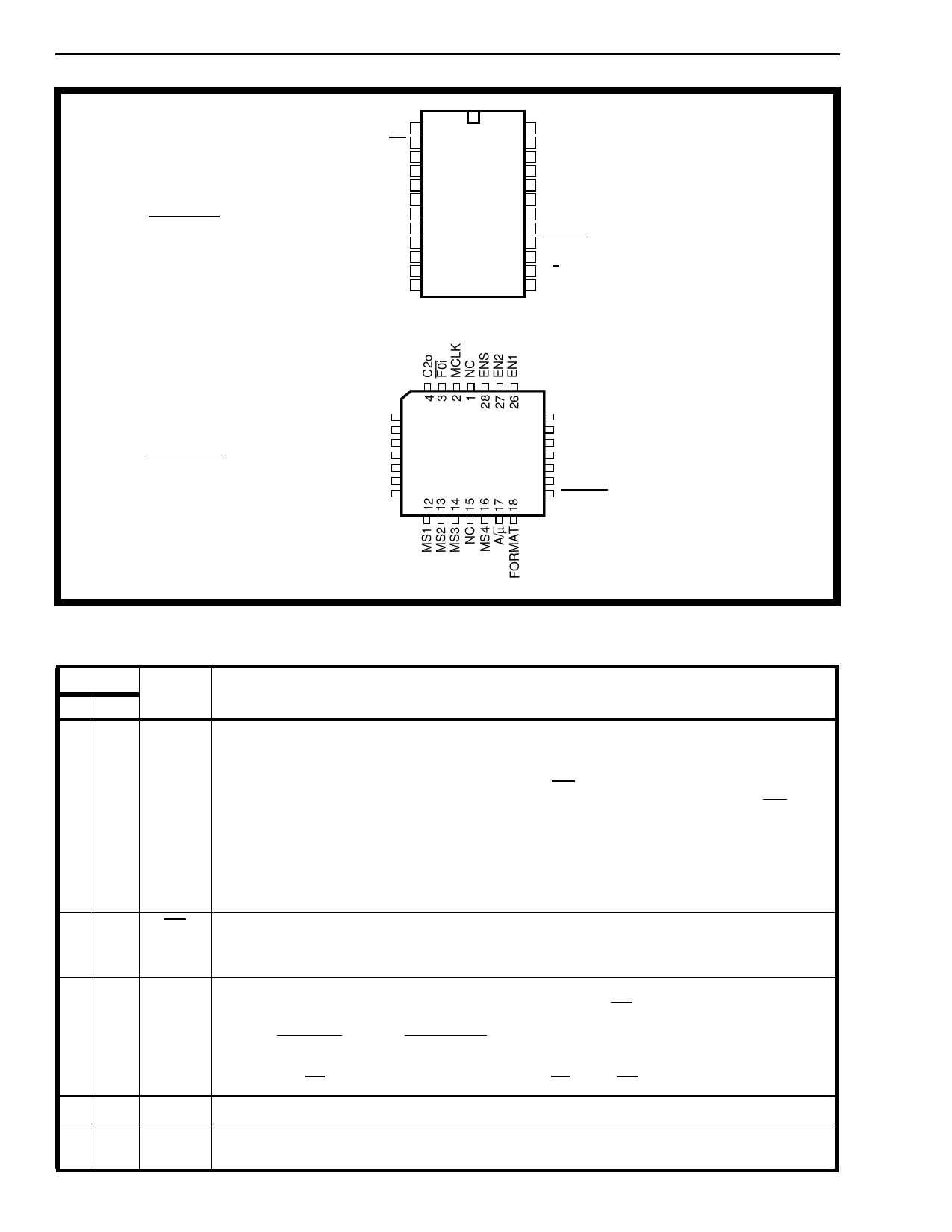
MT9125
24 PIN PDIP
Preliminary Information
MCLK 1
F0i 2
C2o 3
DSTo 4
DSTi 5
BCLK 6
VSS 7
ENB2 8
ENB1 9
MS1 10
MS2 11
MS3 12
24 ENS
23 EN2
22 EN1
21 ADPCMo
20 ADPCMi
19 ENA
18 VDD
17 IC
16 PWRDN
15 FORMAT
14 A/µ
13 MS4
28 PIN PLCC
DSTo 5
•
25 ADPCMo
DSTi 6
24 ADPCMi
BCLK 7
23 ENA
VSS 8
22 VDD
NC 9
21 NC
ENB2 10
20 IC
ENB1 11
19 PWRDN
Pin Description
Figure 2 - Pin Connections
Pin #
DIP PLCC
12
Name
MCLK
Description
Master Clock input. This 4.096 MHz clock is used as an internal master clock and must be
provided during both ST-BUS and SSI modes of operation. This is a TTL level input.
In ST-BUS mode the MCLK input (also known as C4i in ST-BUS terms) is derived from the
synchronous 4.096 MHz clock available from the layer 1 transceiver device. The C4i clock,
input to MCLK, is used in this mode as both the internal master clock and for deriving the
C2o output clock and EN1/EN2 output enable strobes.
23
34
45
56
F0i
C2o
DSTo
DSTi
In SSI mode a 4.096 MHz master clock must be derived from an external source. This
master clock may be asynchronous relative to the 8 kHz frame reference.
Frame alignment input pulse for ST-BUS interface operation. This input should be tied low
if ST-BUS operation is not required.
This is a TTL level input.
2.048MHz Clock output for ST-BUS applications. This clock is MCLK divided by 2 and
inverted. The C2o output activity state is governed by the F0i input pin condition.
F0i input
C2o output
VSS
VDD
Active F0i strobe
disabled (SSI mode automatically activated)
enabled
enabled and aligned to F0i due to C4i input at MCLK
Serial PCM octet output stream. Refer to the serial timing diagram of Figure 12.
Serial PCM octet input data stream. Refer to the serial timing diagram of Figure 12.
This is a TTL level input.
8-74
Share Link: 