LH28F160BJHE-TTL90 데이터 시트보기 (PDF) - Sharp Electronics
부품명
상세내역
일치하는 목록
LH28F160BJHE-TTL90 Datasheet PDF : 47 Pages
| |||
SHARP
LHFl6504
9
1
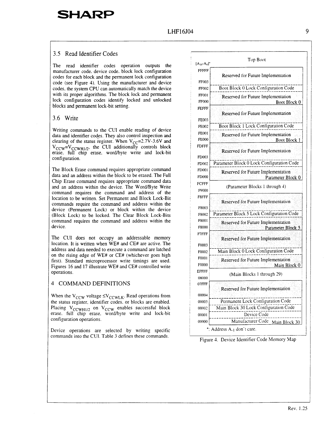
3.5 Read Identifier Codes
The read identifier codes operation outputs the
manufacturer code. device code. block lock configuration
codes for each block and the permanent lock configuration
code (see Figure 4). Using the manufacturer and device
codes. the system CPU can automatically match the device
with its proper algorithms. The block lock and permanent
lock configuration codes identify locked and unlocked
blocks and permanent lock-bit settin:.
3.6 Write
Writing commands to the CUI enable reading of device
data and identifier codes. They also control inspection and
clearing of the status register. When V&=2.7V-3.6V and
V CCW=VCCWHIR) the CUI additionally controls block
erase. full chip erase, word/byte write and lock-bit
configuration.
The Block Erase command requires appropriate command
data and an address within the block to be erased. The Full
Chip Erase command requires appropriate command data
and an address within the device. The Word/Byte Write
command requires the command and address of the
location to be written. Set Permanent and Block Lock-Bit
commands require the command and address within the
zlevice (Permanent Lock) or block within the device
iBlock Lock) to be locked. The Clear Block Lock-Bits
:ommand requires the command and address within the
levice.
lhe CUI does not occupy an addressable memory
ocation. It is written when WE# and CE# are active. The
iddress and data needed to execute a command are latched
)n the rising edge of WE# or CE# (whichever goes high
‘First). Standard microprocessor write timings are used.
?gures 16 and 17 illustrate WE# and CE# controlled write
operations.
t COMMAND DEFINITIONS
Nhen the VCcw voltage IV,,,,.
Read operations from
he status register, identifier codes. or blocks are enabled.
‘lacing VCCWH,,2 on VCCw enables successful block
:rase. full chip erase. word/byte write and lock-bit
configuration operations.
device operations are selected by writing specific
ommands into the CUI. Table 3 defines these commands.
FFFFFf
I Reserved for Future Implementation
FFrm _______________-----------------------
I
FFOOZ ____B__o_o_t _B--l-o-c--k---0---L~o~c~k~~C~o~n~l~ig~u~r~a~ti~o~n~C~o&
FFOOI Reserved for Future Implementation
FFOOO
Boot Block 0
FEFFF
Reserved for Future Implementation
FE003 _____________
-------
----------
------
FE002
Boot Block 1 Lock Conlieuration Code
__________---------------_----_-
FDOOl
FDmil
Reserved for Future Implementation
Parameter Block 0
.,.I-- FCFFF;
FW,-!il
!
(Parameter Blocks I through -I)
Reserved for Future Implementation
FXOO? _--_-______-__-___-_------------------
-
F8001 Reserved for Future ImpIementation
F8000
Parameter Block 5
F7FFF
Reserved for Future Implementation
FOO03
EFFFF:
(Main Blocks 1 through 29)
“----
I:::_::_:::: 07FFF
Reserved for Future Implementation
00004
00003
Permanent Lock Conligrration Code
OOOO? Main Block 30 Lock Configuration Code
0000 I ________________D_e_v_ic_e---C--o--d--e---------
00000
Manufacturer Code Main Block j[J
*: Address A.1 don‘t care.
Figure 4. Device Identifier Code Memory .Map
Rev. 1.25
Share Link: 