U632H16 데이터 시트보기 (PDF) - Zentrum Mikroelektronik Dresden AG
부품명
상세내역
일치하는 목록
U632H16 Datasheet PDF : 14 Pages
| |||
U632H16
PowerStore 2K x 8 nvSRAM
Features
F Packages: PDIP28 (300 mil) auto matically on power up. The
PDIP28 (600 mi) U632H16 combines the high perfor-
F High-performance CMOS no n-
SOP28 (300 mil) mance and ease of use of a fast
volatile stati c RAM 2048 x 8 bits
F 25, 35 and 45 ns Ac cess Times Description
F 12, 20 and 25 ns Output Enable
SRAM with n onvolatile data inte-
grit y.
STORE cycles also may be initiated
Access Times
F ICC = 15 mA at 200 ns Cy cle
Tim e
F Auto matic S TORE to EEPROM
on Po wer Do wn usi ng external
capacito r
F Hardware o r So ftware initiated
STORE
(STORE Cy cle Time < 10 ms )
F Auto matic S TORE Timing
F 105 STORE cycles to EEPROM
F 10 years data retentio n in
EEPROM
F Auto matic RECALL on Po wer Up
F Sof tware RECALL I nitiatio n
(RECALL Cy cle Time < 20µs)
F Unlimited RECALL cy cles from
EEPROM
F Single 5 V± 10 % Operation
F Operating temperature rang es:
0 to 70 °C
-40 to 85 °C
The U632H16 has two separate
modes of o peration: SRAM mode
and no nv olatile mode. In SRAM
mode, the memo ry operates as an
ordinary st atic RA M. In nonvolatile
operation, data is trans ferred in
parallel fro m SRAM to EEPROM or
fro m EEPROM to SRAM. In this
mode SRAM fu nctio ns are disab-
led.
The U632H16 is a fast s tatic RAM
(25, 35, 45 ns), w ith a nonvolatile
electr ically erasable PROM
(EEPROM) element inco rpo rated
in each static m emory cell. The
SRAM can be read and wri tten an
unlimited number of ti mes, while
independent nonvolatile data resi-
des in EEPROM. Data trans fers
fro m the SRAM to the EEPROM
(the STORE operatio n) take place
auto matically upo n power do wn
under us er contro l via a softw are
sequence or via a single pin (HSB).
Once a STORE cy cle is init iated,
furt her input or outpu t are disabled
until the cycle is co mpleted.
Because a sequence of addresses
is used for STORE initiation, it is
imp ortant that no o ther read o r write
access es interv ene in the sequence
or the sequence will be abo rted.
RECALL cycles may also be initia-
ted by a software sequence.
Internally, RECALL is a two step
procedure. First, the SRAM data is
cleared and seco nd, the nonvolatile
information is tr ans ferred into the
SRAM cells.
The RECALL operation in no way
alters the data in the EEPROM
cells. The no nvolatile data can be
recalled an unlimited nu mber of
ti me s .
F CECC 90000 Quality Standard usi ng charge stored in an external
F ESD ch aracteri zatio n according 100 µF capaci tor. Trans fers fro m
MIL STD 883C M3015.7-HBM
the EEPROM to the SRAM (the
(classific atio n see IC Code Num- RECALL operation) take place
b er s )
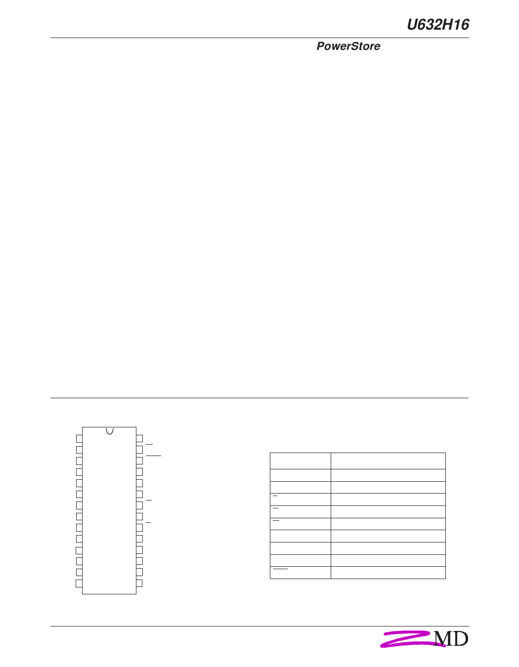
Pin Configuration
VCA P
n.c.
A7
A6
A5
A4
A3
A2
A1
A0
DQ0
DQ1
DQ2
VSS
1
28
2
27
3
26
4
25
5
24
6
23
7 PDIP 22
8 SOP 21
9
20
10
19
11
18
12
17
13
16
14
15
VCCX
W
HSB
A8
A9
n.c .
G
A10
E
DQ7
DQ6
DQ5
DQ4
DQ3
Pin Description
Signal Name
A0 - A10
DQ0 - DQ7
E
G
W
VCCX
VSS
VCAP
HSB
Signal Description
Addres s Inputs
Data In/Out
Chip En able
Output Enable
Write Enable
Power Supp ly Volt age
Ground
Capacit or
Hardware Controlle d Store/Busy
Top View
December 12, 1997
1
Share Link: 