W147G 데이터 시트보기 (PDF) - Cypress Semiconductor
부품명
상세내역
일치하는 목록
W147G Datasheet PDF : 12 Pages
| |||
PRELIMINARY
W147G
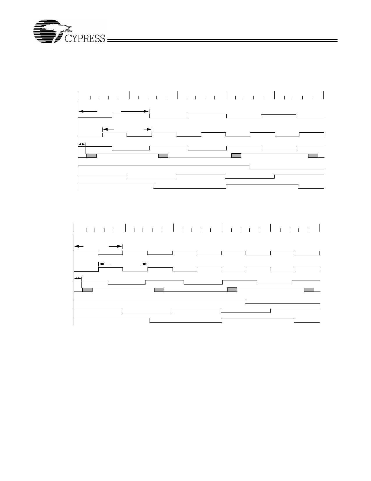
Offsets Among Clock Signal Groups
Figure 2 and Figure 3 represent the phase relationship among
the different groups of clock outputs from W147G when it is
providing a 66-MHz CPU clock and a 100-MHz CPU clock,
respectively. It should be noted that when CPU clock is oper-
ating at 100 MHz, CPU clock output is 180 degrees out of
phase with SDRAM clock outputs.
0 ns
10 ns
20 ns
30 ns
40 ns
CPU 66-MHz
C PU 66 Pe riod
SDRAM 100-MHz
3V66 66-MHz
PCI 33-MHz
REF 14.318-MHz
USB 48-MHz
APIC 33-MHz
Hub-PCI
SDRAM 100 Period
Figure 2. Group Offset Waveforms (66-MHz CPU Clock)
0 ns
10 ns
20 ns
30 ns
40 ns
CPU 100-MHz
CPU 100 Period
SDRAM 100-MHz
3V66 66-MHz
PCI 33-MHz
REF 14.318-MHz
USB 48-MHz
APIC 33-MHz
Hub-PCI
SD R A M 10 0 P e rio d
Figure 3. Group Offset Waveforms (100-MHz CPU Clock)
4
Share Link: 