NJG1720PB1 데이터 시트보기 (PDF) - Japan Radio Corporation
부품명
상세내역
일치하는 목록
NJG1720PB1 Datasheet PDF : 21 Pages
| |||
NJG1720PB1
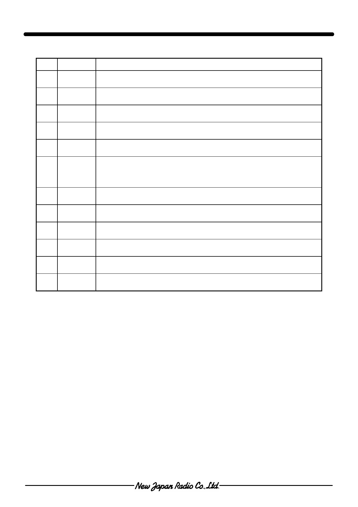
nTERMINAL INFORMATION
No. Symbol
Description
1
LNAOUT
Output terminal. This is the power supply terminal of the LNA. Please use
inductor(L5) to connect power supply.(Please see test circuit.)
2
VCTL
Control voltage input terminal. This terminal is set to Full band and CD
band to select.
3 LNAIN2 Input terminal of full band. The DC blocking capacitor is not required.
4 LNAIN1 Input terminal of CD band. The DC blocking capacitor is not required.
5
GND Ground terminal (0V)
IF signal output terminal. The IF signal is output through external matching
6
IFOUT
circuit connected to this terminal. Please connect inductances C4, L9 and
power supply as shown in test circuits, since this terminal is also the
terminal of mixer power supply.
7
VLO
Power supply terminal for local amplifier. Please place L8 shown in test
circuits at very close to this terminal.
8
GND Ground terminal (0V)
9
LOIN
Local signal input terminal to local amplifier. An external matching circuit is
required.
10
GND Ground terminal (0V)
11
MIXIN RF signal input terminal to mixer. An external matching circuit is required.
12
VINV Power supply terminal of the inverter circuit.
NOTE:
1) Ground terminal (5, 8, 10pin) should be connected to ground plane by multiple via holes
for good grounding.
-5-
Share Link: 