NJG1720PB1 데이터 시트보기 (PDF) - Japan Radio Corporation
부품명
상세내역
일치하는 목록
NJG1720PB1 Datasheet PDF : 21 Pages
| |||
NJG1720PB1
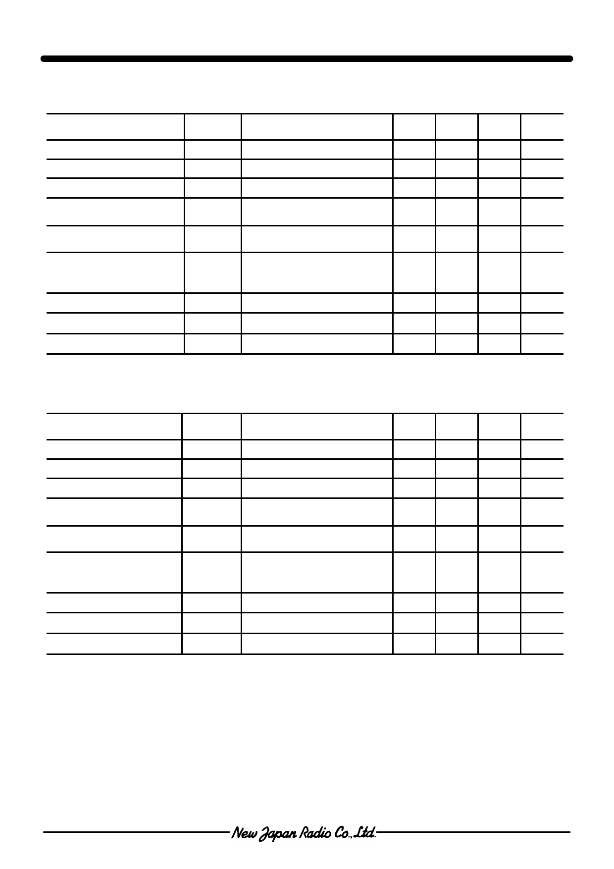
nELECTRICAL CHARACTERISTICS (LNA1 RF CHARACTERISTICS)
GENERAL CONDITIONS: Ta=+25°C, Zs=Zl=50Ω, VDD=VINV=2.8V, VCTL=0V,
with test circuit
PARAMETER
SYMBOL
CONDITIONS
MIN TYP MAX UNITS
Operating Frequency
Small Signal Gain
Gain Flatness
Noise Figure
Pin at 1dB Gain
Compression point
Input 3rd Order
Intercept Point
Isolation
freq
Gain
Gflat
NF
P-1dB(IN)
IIP3
ISO
810
16.5
freq=810~843MHz
-
Loss of PCB and connector
are excluded
-
-21.0
2 tone offset
frequency=100kHz,
PRF=-36dBm
freq=675.15 to 750.15MHz
-10.0
25
830
17.5
0.5
1.5
-18.0
-7.0
30
843
19.0
1.0
1.7
-
-
-
MHz
dB
dB
dB
dBm
dBm
dB
Input VSWR
Output VSWR
VSWRI
VSWRo
-
1.5 2.0
-
-
1.5 2.0
-
nELECTRICAL CHARACTERISTICS (LNA2 RF CHARACTERISTICS)
GENERAL CONDITIONS: Ta=+25°C, Zs=Zl=50Ω, VDD=VINV=2.8V, VCTL=2.4V
with test circuit
PARAMETER
SYMBOL
CONDITIONS
MIN TYP MAX UNITS
Operating Frequency
Small Signal Gain
Gain Flatness
Noise Figure
Pin at 1dB Gain
Compression point
Input 3rd Order
Intercept Point
Isolation
freq
Gain
Gflat
NF
P-1dB(IN)
IIP3
ISO
810
16.5
freq=810~885MHz
-
Loss of PCB and connector
are excluded
-
-21.0
2 tone offset
frequency=100kHz,
PRF=-36dBm
freq=675.15 to 750.15MHz
-10.0
25
840
17.5
0.5
1.5
-18.0
-7.0
30
885
18.5
1.2
1.7
-
-
-
MHz
dB
dB
dB
dBm
dBm
dB
Input VSWR
Output VSWR
VSWRI
VSWRo
-
1.5 2.0
-
-
1.5 2.0
-
-3-
Share Link: 