IDT74FCT543DTSOG 데이터 시트보기 (PDF) - Integrated Device Technology
부품명
상세내역
일치하는 목록
IDT74FCT543DTSOG Datasheet PDF : 7 Pages
| |||
IDT74FCT543AT/CT/DT
FAST CMOS OCTAL LATCHED TRANSCEIVER
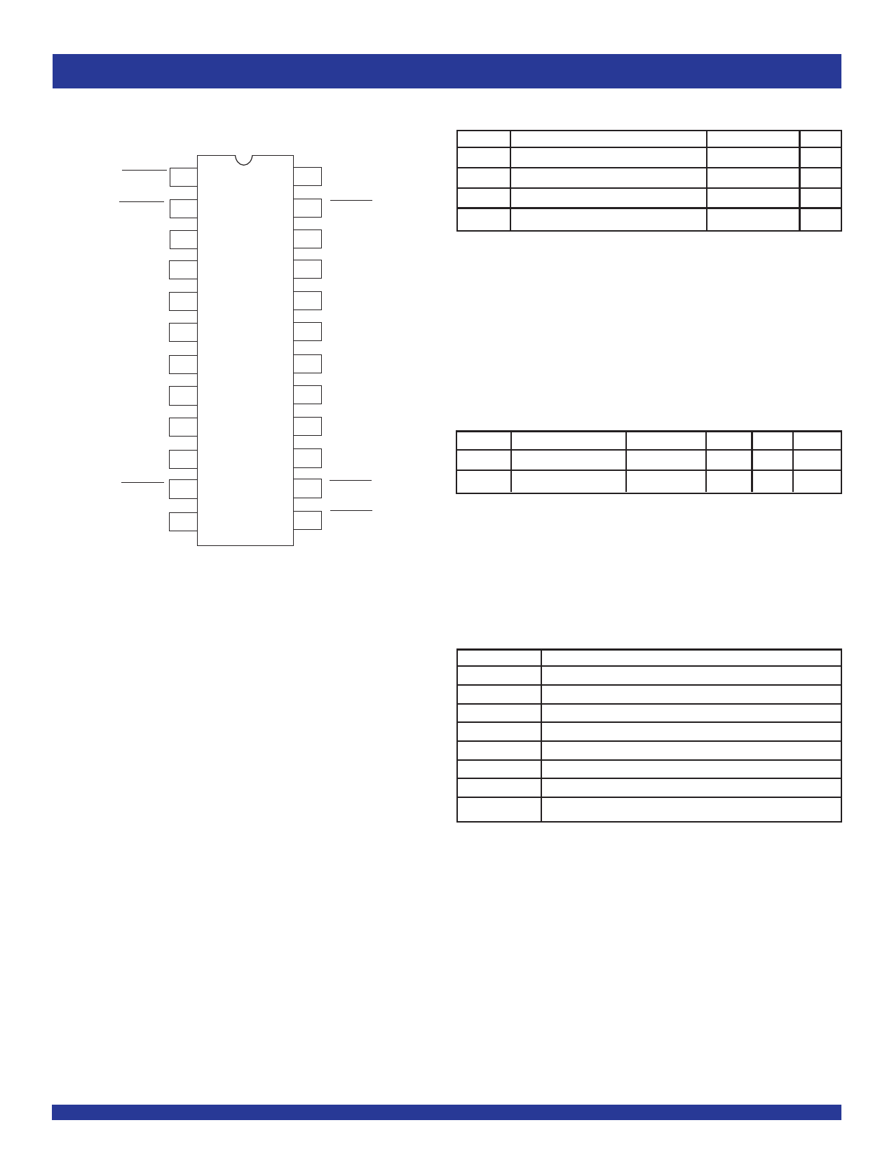
PIN CONFIGURATION
LEBA 1
OEBA 2
A0 3
A1 4
A2 5
A3 6
A4 7
A5 8
A6 9
A7 10
CEAB 11
GND 12
24
VCC
23 CEBA
22
B0
21
B1
20
B2
19
B3
18
B4
17
B5
16
B6
15
B7
14 LEAB
13 OEAB
SOIC/ QSOP
TOP VIEW
INDUSTRIAL TEMPERATURE RANGE
ABSOLUTE MAXIMUM RATINGS(1)
Symbol
Description
Max
Unit
VTERM(2) Terminal Voltage with Respect to GND
–0.5 to +7
V
VTERM(3) Terminal Voltage with Respect to GND –0.5 to VCC+0.5 V
TSTG Storage Temperature
–65 to +150
°C
IOUT DC Output Current
–60 to +120 mA
NOTES:
1. Stresses greater than those listed under ABSOLUTE MAXIMUM RATINGS may cause
permanent damage to the device. This is a stress rating only and functional operation
of the device at these or any other conditions above those indicated in the operational
sections of this specification is not implied. Exposure to absolute maximum rating
conditions for extended periods may affect reliability. No terminal voltage may exceed
Vcc by +0.5V unless otherwise noted.
2. Inputs and Vcc terminals only.
3. Output and I/O terminals only.
CAPACITANCE (TA = +25°C, F = 1.0MHz)
Symbol
Parameter(1)
Conditions Typ. Max. Unit
CIN
Input Capacitance
VIN = 0V
6
10 pF
COUT
Output Capacitance VOUT = 0V
8
12 pF
NOTE:
1. This parameter is measured at characterization but not tested.
PIN DESCRIPTION
Pin Names
Description
OEAB
A-to-B Output Enable Input (Active LOW)
OEBA
B-to-A Output Enable Input (Active LOW)
CEAB
A-to-B Enable Input (Active LOW)
CEBA
B-to-A Enable Input (Active LOW)
LEAB
A-to-B Latch Enable Input (Active LOW)
LEBA
B-to-A Latch Enable Input (Active LOW)
A0–A7
A-to-B Data Inputs or B-to-A 3-State Outputs
B0–B7
B-to-A Data Inputs or A-to-B 3-State Outputs
2
Share Link: 