IDT71V424YL 데이터 시트보기 (PDF) - Integrated Device Technology
부품명
상세내역
일치하는 목록
IDT71V424YL Datasheet PDF : 9 Pages
| |||
IDT71V424YS, IDT71V424YL, 3.3V CMOS Static RAM
4 Meg (512K x 8-bit)
Commercial and Industrial Temperature Ranges
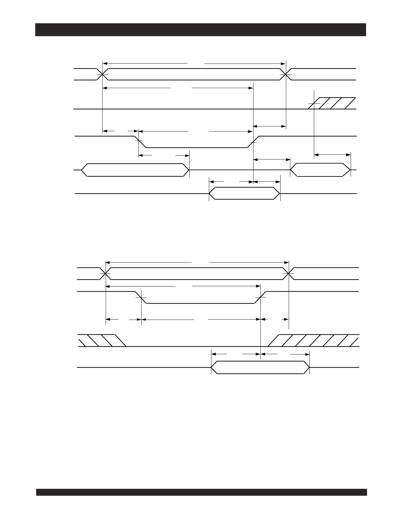
Timing Waveform of Write Cycle No. 1 (WE Controlled Timing)(1, 2, 4)
ADDRESS
tWC
tAW
C
S
WE
DATAOUT
DATAIN
tWR
tAS
tWP(2)
tWHZ (5)
(3)
HIGH IMPEDANCE
tDW
tOW (5)
tDH
DATAIN VALID
tCHZ (5)
(3)
6468 drw 08
Timing Waveform of Write Cycle No. 2 (CS Controlled Timing)(1, 4)
ADDRESS
C
S
tWC
tAW
tAS
tCW
tWR
WE
DATAIN
tDW
tDH
DATAIN VALID
6468 drw 09
NOTES:
1. A write occurs during the overlap of a LOW CS and a LOW WE.
2. OE is continuously HIGH. During a WE controlled write cycle with OE LOW, tWP must be greater than or equal to tWHZ + tDW to allow the I/O drivers to turn off and
data to be placed on the bus for the required tDW. If OE is HIGH during a WE controlled write cycle, this requirement does not apply and the minimum write pulse
is the specified tWP.
3. During this period, I/O pins are in the output state, and input signals must not be applied.
4. If the CS LOW transition occurs simultaneously with or after the WE LOW transition, the outputs remain in a high impedance state. CS must be active during the tCW
write period.
5. Transition is measured ±200mV from steady state.
6.472
Share Link: 