IDT71V424YL 데이터 시트보기 (PDF) - Integrated Device Technology
부품명
상세내역
일치하는 목록
IDT71V424YL Datasheet PDF : 9 Pages
| |||
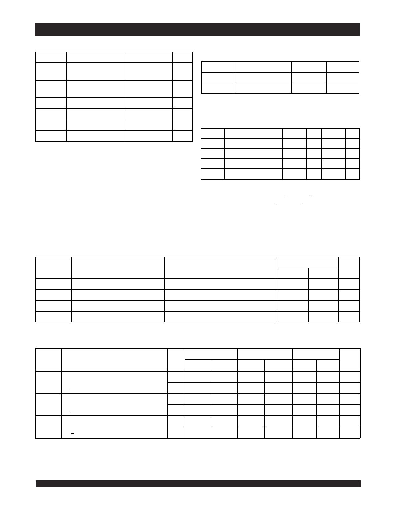
IDT71V424YS, IDT71V424YL, 3.3V CMOS Static RAM
4 Meg (512K x 8-bit)
Absolute Maximum Ratings(1)
Symbol
Rating
Value
Unit
VDD
Supply Voltage Relative
-0.5 to +4.6
V
to VSS
VIN, VOUT Terminal Voltage Relative -0.5 to VDD+0.5
V
to VSS
TBIAS
Temperature Under Bias
-55 to +125
oC
TSTG
Storage Temperature
-55 to +125
oC
PT
Power Dissipation
1
W
IOUT
DC Output Current
50
mA
NOTE:
6468 tbl 04
1. Stresses greater than those listed under ABSOLUTE MAXIMUM RATINGS may
cause permanent damage to the device. This is a stress rating only and
functional operation of the device at these or any other conditions above those
indicated in the operational sections of this specification is not implied. Exposure
to absolute maximum rating conditions for extended periods may affect
reliability.
Commercial and Industrial Temperature Ranges
Recommended Operating
Temperature and Supply Voltage
Grade
Commercial
Industrial
Temperature
0°C to +70°C
–40°C to +85°C
VSS
VDD
0V
See Below
0V
See Below
6468 tbl 05
Recommended DC Operating
Conditions
Symbol
Parameter
Min. Typ. Max. Unit
VDD Supply Voltage
3.0
3.3
3.6
V
VSS Ground
0
0
0
V
VIH Input High Voltage
2.0
____ VDD+0.3(1) V
VIL Input Low Voltage
-0.3(2)
____
0.8
V
NOTES:
1. VIH (max.) = VDD+2V a.c. (Pulse Width < 5ns) for I < 20mA.
2. VIL (min.) = –2V a.c. (Pulse Width < 5ns) for I < 20mA.
6468 tbl 06
DC Electrical Characteristics
(VDD = Min. to Max., Commercial and Industrial Temperature Ranges)
IDT71V424
Symbol
Parameter
Test Condition
Min.
Max. Unit
|ILI|
Input Leakage Current
|ILO|
Output Leakage Current
VDD = Max., VIN = VSS to VDD
VDD = Max., CS = VIH, VOUT = VSS to VDD
___
5
µA
___
5
µA
VOL
Output Low Voltage
IOL = 8mA, VDD = Min.
___
0.4
V
VOH
Output High Voltage
IOH = -4mA, VDD = Min.
2.4
___
V
DC Electrical Characteristics(1, 2, 3)
(VDD = Min. to Max., VLC = 0.2V, VHC = VDD – 0.2V)
71V424YS/YL 10
Symbol
Parameter
Com'l.
Ind.(5)
71V424YS/YL 12
Com'l.
Ind.(5)
6468 tbl 07
71V424YS/YL 15
Unit
Com'l. Ind.(5)
ICC
Dynamic Operating Current
S
CS < VLC, Outputs Open, VDD = Max., f = fMAX(4) L
180
165
180
___
170
155
170
155
160
160 mA
145
145 mA
ISB
Dynamic Standby Power Supply Current
S
CS > VHC, Outputs Open, VDD = Max., f = fMAX(4) L
60
55
60
___
55
50
55
50
50
mA
50
45
45
mA
ISB1
Full Standby Power Supply Current (static)
CS > VHC, Outputs Open, VDD = Max., f = 0(4)
S
L
20
10
20
___
20
10
NOTES:
1. All values are maximum guaranteed values.
2. All inputs switch between 0.2V (Low) and VDD - 0.2V (High).
3. Power specifications are preliminary.
4. fMAX = 1/tRC (all address inputs are cycling at fMAX); f = 0 means no address input lines are changing.
5. Standard power 10ns (S10) speed grade only.
20
20
20
mA
10
10
10
mA
6468 tbl 08
6.432
Share Link: 