MAX1203ACAP(1998) 데이터 시트보기 (PDF) - Maxim Integrated
부품명
상세내역
일치하는 목록
MAX1203ACAP Datasheet PDF : 24 Pages
| |||
5V, 8-Channel, Serial, 12-Bit ADCs
with 3V Digital Interface
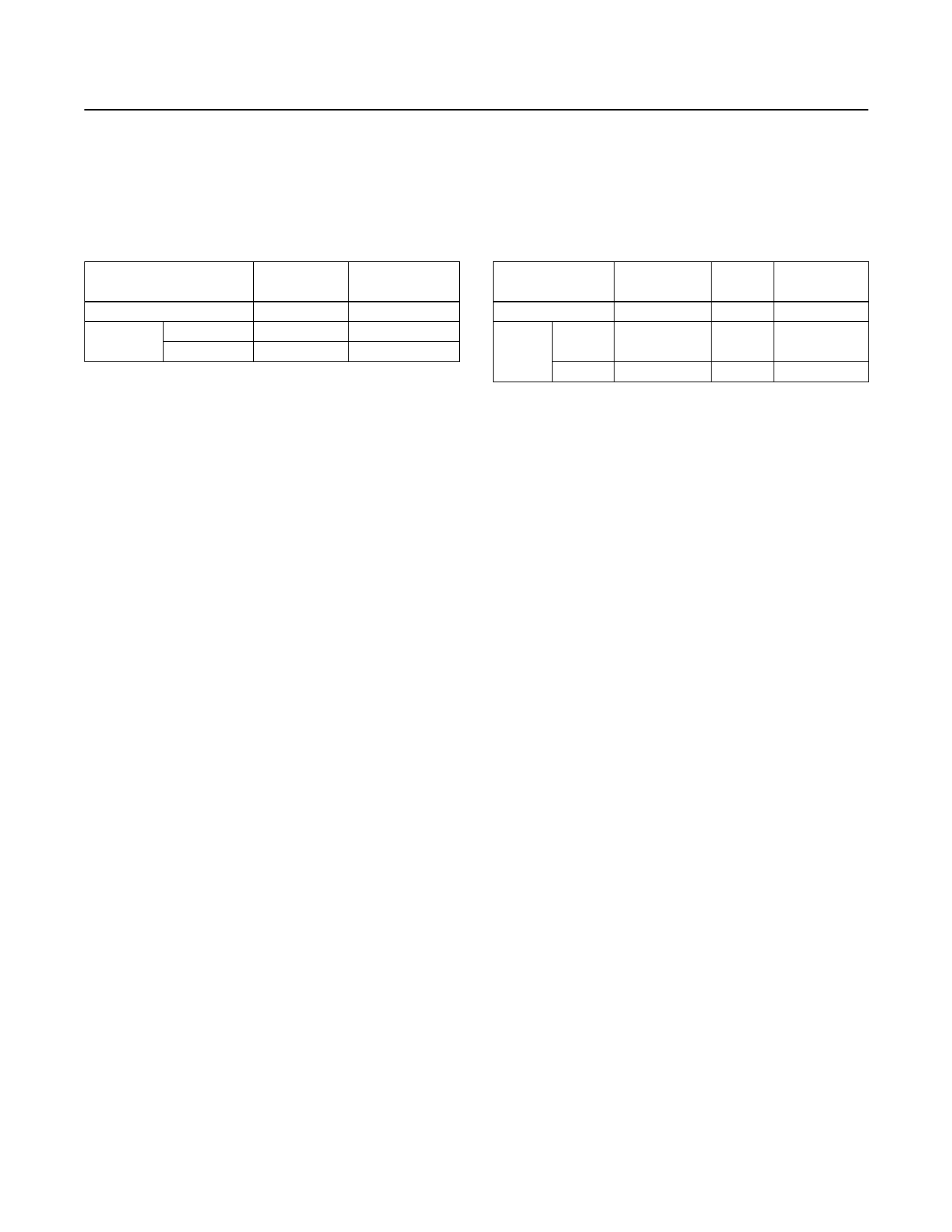
Table 1a. Unipolar Full Scale and Zero
Scale
REFERENCE
ZERO
SCALE
FULL SCALE
Internal
0V
at REFADJ
0V
External
at REF
0V
+4.096V
VREFADJ x A*
VREF
*A = 1.68 for the MAX1202, 1.64 for the MAX1203.
Table 1b. Bipolar Full Scale, Zero Scale,
and Negative Full Scale
REFERENCE
NEGATIVE
FULL SCALE
ZERO
SCALE
FULL SCALE
Internal
-4.096V / 2
0V +4.096V / 2
at
-1/2 VREFADJ
External REFADJ
x A*
0V
+1/2 VREFADJ
x A*
at REF
-1/2 VREF
0V
+1/2 VREF
*A = 1.68 for the MAX1202, 1.64 for the MAX1203.
Input Bandwidth
The ADC’s input tracking circuitry has a 4.5MHz
small-signal bandwidth. Therefore it is possible to digi-
tize high-speed transient events and measure periodic
signals with bandwidths exceeding the ADC’s sampling
rate by using undersampling techniques. To avoid
high-frequency signals being aliased into the frequency
band of interest, anti-alias filtering is recommended.
Analog Input Range and Input Protection
Internal protection diodes, which clamp the analog
inputs to VDD and VSS, allow the analog input pins to
swing from (VSS - 0.3V) to (VDD + 0.3V) without dam-
age. However, for accurate conversions near full scale,
the inputs must not exceed VDD by more than 50mV, or
be lower than VSS by 50mV.
If the analog input exceeds 50mV beyond the sup-
plies, do not forward bias the protection diodes of
off-channels more than 2mA.
The full-scale input voltage depends on the voltage at
REF (Tables 1a and 1b).
Quick Look
Use the circuit of Figure 5 to quickly evaluate the
MAX1202/MAX1203’s analog performance. The
MAX1202/MAX1203 require a control byte to be written
to DIN before each conversion. Tying DIN to +3V feeds
in control byte $FF hex, which triggers single-ended
unipolar conversions on CH7 in external clock mode
without powering down between conversions. In exter-
nal clock mode, the SSTRB output pulses high for one
clock period before the most significant bit of the 12-bit
conversion result shifts out of DOUT. Varying the ana-
log input to CH7 alters the sequence of bits from
DOUT. A total of 15 clock cycles per conversion is
required. All SSTRB and DOUT output transitions occur
on SCLK’s falling edge.
How to Start a Conversion
Clocking a control byte into DIN starts conversion on
the MAX1202/MAX1203. With CS low, each rising edge
on SCLK clocks a bit from DIN into the MAX1202/
MAX1203’s internal shift register. After CS falls, the first
logic “1” bit defines the control byte’s MSB. Until this
first “start” bit arrives, any number of logic “0” bits can
be clocked into DIN with no effect. Table 2 shows the
control-byte format.
The MAX1202/MAX1203 are fully compatible with
SPI/MICROWIRE devices. For SPI, select the correct
clock polarity and sampling edge in the SPI control reg-
isters: set CPOL = 0 and CPHA = 0. MICROWIRE and
SPI both transmit and receive a byte at the same time.
Using the Typical Operating Circuit, the simplest soft-
ware interface requires only three 8-bit transfers to per-
form a conversion (one 8-bit transfer to configure the
ADC, and two more 8-bit transfers to clock out the
12-bit conversion result).
______________________________________________________________________________________ 11
Share Link: 